
Digital Circuit
Index 14
DDS_DIGITAL_VFO
Published:2009/6/23 1:58:00 Author:May
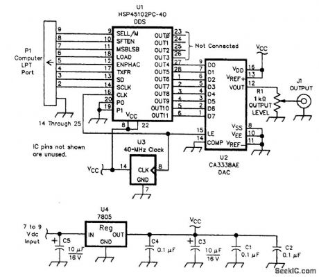
The DDS chip (U1) generates a data stream that is converted by D/A converter U2 into a sine wave. U1 is programmed via the input from P1, from the LPT port of an IBM PC. The system uses a 40-MHz TTL output clock module. (View)
View full Circuit Diagram | Comments | Reading(1148)
FET_VXO_CIRCUIT
Published:2009/6/23 1:49:00 Author:May
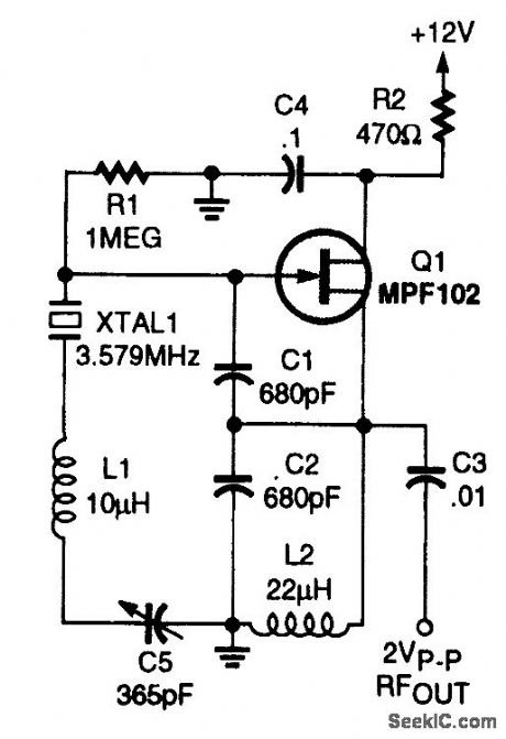
An MPF 102 is used in a Colpitts-type oscilla-tor in order to pull the crystal frequency slightly. (View)
View full Circuit Diagram | Comments | Reading(0)
DITHERIZER
Published:2009/6/22 23:54:00 Author:May
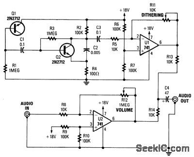
In digital audio, a noise signal of amplitude less than one significant bit is often added to the au-dio to reduce the quantizing effect and improve the audio quality by trading digital noise for ana-log noise, which does not have the harsh sound. This circuit consists of a noise generator to add a low level of noise to an analog signal to be digitized, or an analog signal from a digital source. (View)
View full Circuit Diagram | Comments | Reading(0)
SINGLE_CHIP_MESSAGE_SYSTEM
Published:2009/6/22 23:35:00 Author:May
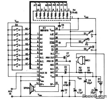
The ISD1016 is a complete analog audio record/playback system on a chip. The analog signal is sampled and the samples stored in an EEPROM as analog levels. Upon playback, the analog data is read out and amplified. Up to 16 seconds of data(audio)can be stored. (View)
View full Circuit Diagram | Comments | Reading(0)
FREQUENCY_DOUBLER
Published:2009/6/22 23:05:00 Author:May
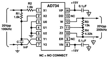
An Analog Devices AD734 four-quadrant analog multiplier is used as a frequency doublen. (View)
View full Circuit Diagram | Comments | Reading(0)
PRINTER_PORT
Published:2009/6/22 22:55:00 Author:May
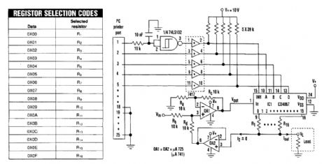
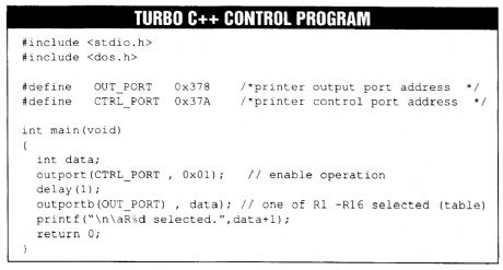
A 16-step programmable current generator can be modified so that it's controllable by a printer port. This is done by switching the resistor connected between the output of the generator's OA1 op amp and the input of OA2. The CMOS single 16-channel analog multiplexer (ICl) chooses one resis-tor at a time, in accordance with the code sent by the printer port through four of its eight data-out-put lines (pins 2 to 9). In addition, one control line (pin 1) is used to enable the operation. As a result, 16 outputs can be selected by a 4-bit word (the table shows the relationship between data word and selected resistor).The following must be fulfilled in order for the circuit to work as a true current generator:
R2×Rd-Rb×Rc =0
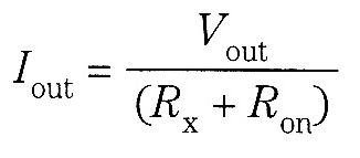
The smaller the resistors' tolerance (especially RI through R16), the greater the output resis-tance of the generator.Because the OA2 is connected as a repeater, the current I2 = O, and only the load current flows through one of the RI through R16 resistors. Therefore:
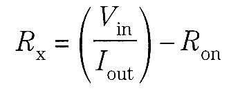
where Vout=Vin;X=1…16;and Ron≤150Ω(for VDD=10 V) is the resistance of one analog switch(CD4067)in conduction Therefore,the values of resistors R1 through R16 can be inferred from the needed currents∶
The Turbo c++ program also controls the current through the load
(View)
View full Circuit Diagram | Comments | Reading(1483)
TELEPHONE_AUDIO_INTERFACE
Published:2009/6/22 22:52:00 Author:May
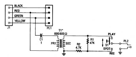
Used to record and play back tapes vla the phone lines,this simple circuit has an audio level switch (S1). (View)
View full Circuit Diagram | Comments | Reading(0)
FREQUENCY_DIVIDER_FOR_MEASUREMENTS
Published:2009/6/22 22:49:00 Author:May
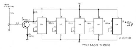
This circuit is meant to be driven by a 1-MHz standard signal of a few volts amplitude. U1 through U5 are 7490 decade counter/divider and produce a division ratio of 100,000:1. Successive divisions of 10 can be tapped off, if desired, between stages. One or more stages can be added for still lower frequencies. (View)
View full Circuit Diagram | Comments | Reading(1948)
PROGRAMMABLE_RESISTOR_CIRCUIT
Published:2009/6/22 22:49:00 Author:May
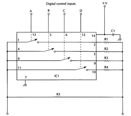
IC1 CD4066 quad bilateral switchC1 0.1-μF capacitorRI 10-kΩ, 1/4-W 5% resistorR2 4.7-kΩ, 1/4-W 5% resistorR3 2.2-kΩ, 1/4-W 5% resistorR4 1-kΩ, 1/4-W 5% resistorR5 1-MΩ, 1/4-W 5% resistor
A programmable resistor can replace a potentiometer or fixed resistor. Remember that the ON resistance of IC1 might have to be taken into account in some applications. (View)
View full Circuit Diagram | Comments | Reading(0)
SCR_INVERTER_AND_TRIGGER_CIRCUIT
Published:2009/6/19 4:47:00 Author:May
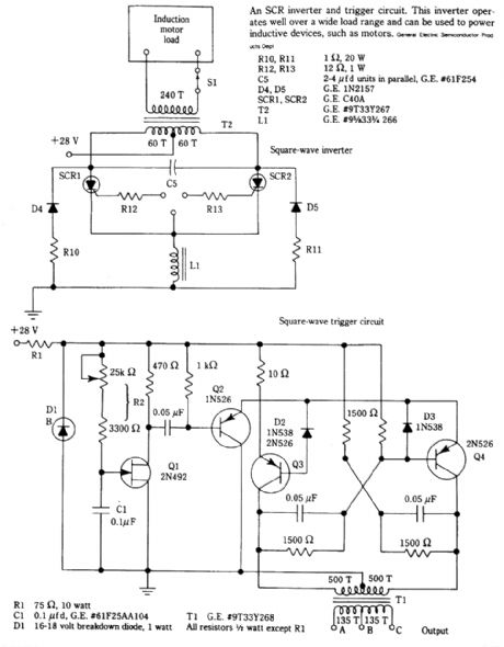
In this circuit, L1 and C5 are used as commutating elements. L1 resonates quency corresponding to the half period of the waveform. (View)
View full Circuit Diagram | Comments | Reading(1058)
SYNC_GATINC_CIRCUIT
Published:2009/6/19 2:36:00 Author:May
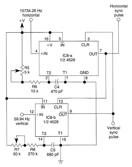
This circuit guarantees that only one type of sync pulse is generated at a time. During vertical sync periods, horizontal sync is disabled. (View)
View full Circuit Diagram | Comments | Reading(804)
74 series digital circuit 74LS465/466 etc eight bus buffer (three state)
Published:2011/5/13 5:10:00 Author:May | Keyword: digital, eight bus buffer, three state
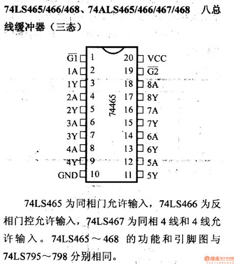
74LS465 is in-phase gatepermiting input, 74LS466 is opposite phase gate controlpermiting input,74LS467 is in-phase four lines and four linespermiting input. The function and pin diagram of 74LS465~468 is seperately same to 74LS795~798. (View)
View full Circuit Diagram | Comments | Reading(1034)
74 series digital circuit 74LS378 74F378 and other six D flip-flop
Published:2011/5/13 5:08:00 Author:May | Keyword: digital, six D flip-flop
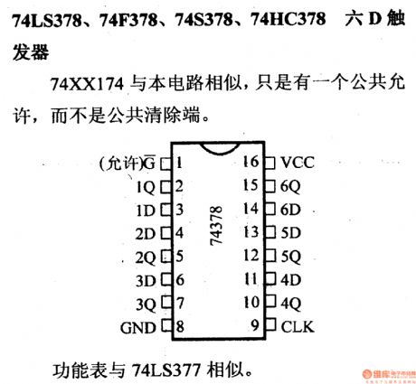
74LS378, 74F378, 74S378, 74HC378 six D trigger74××174 is similar to this circuit. It only has one public permitting but not public clearing end. (View)
View full Circuit Diagram | Comments | Reading(872)
74 series digital circuit 74LS377 and other eight D flip-flop
Published:2011/5/13 5:06:00 Author:May | Keyword: digital, eight D flip-flop
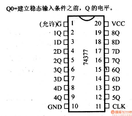
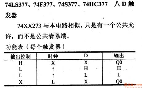
Q0=the level of Q before building stability input condition.74LS377, 74F377, 74S377, 74HC377 eight D trigger74××273 is similar to this circuit. It only has one public permitting but not public clearing end. (View)
View full Circuit Diagram | Comments | Reading(900)
FREQUENCY_DIVIDER_FOR_10_MHz_FREQUENCY_STANDARD
Published:2009/6/19 2:28:00 Author:May
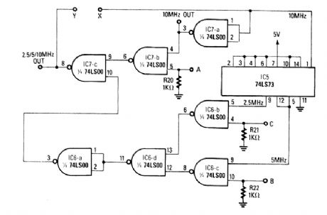
View full Circuit Diagram | Comments | Reading(876)
74 Series digital circuit 74376 four J-K non-flip-flop
Published:2011/5/13 5:02:00 Author:May | Keyword: digital, four J-K, non-flip-flop
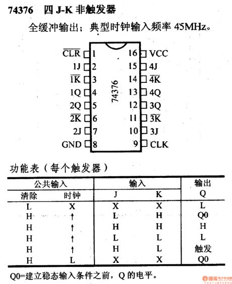
74376 four J-K non-triggerfull buffer output: typical clock input frequency is 45MHz
(View)
View full Circuit Diagram | Comments | Reading(846)
74 Series digital circuit 74S340 74S341 and other eight buffer/line driver (three-state)
Published:2011/5/11 3:57:00 Author:May | Keyword: digital, eight buffer, line driver, three-state
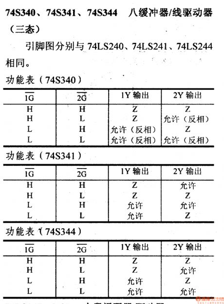
74S340, 74S341, 74S344 eight buffer/line driver (tristate)Their pin diagrams is seperately same as 74LS240, 74LS241, 74LS244.
(View)
View full Circuit Diagram | Comments | Reading(635)
74 Series digital circuit 74298 74LS298 and other 4-bit 2 selects 1 data selector (register output)
Published:2011/5/11 3:58:00 Author:May | Keyword: digital, 4-bit, 2 selection 1, data selector, register output
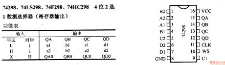
View full Circuit Diagram | Comments | Reading(1135)
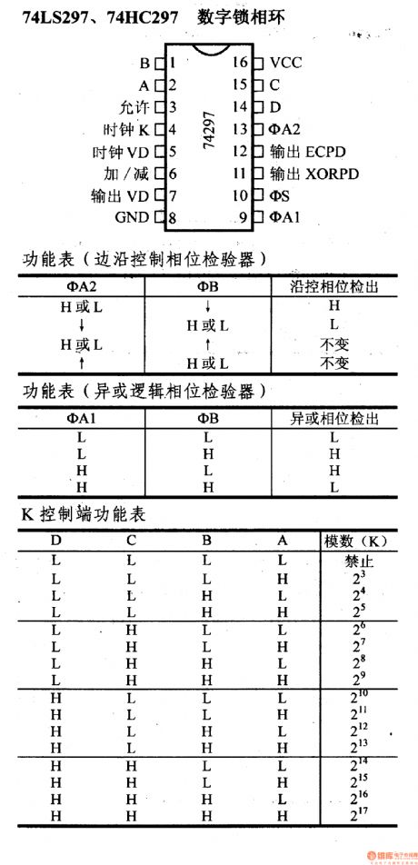
74 series digital circuit 74LS297 74HC297 and other digital phase-locked loop
Published:2011/5/11 3:59:00 Author:May | Keyword: digital, digital phase-locked loop
View full Circuit Diagram | Comments | Reading(1095)
PIN_DIODE_FILTER_SELECTION_CIRCUIT
Published:2009/6/19 1:59:00 Author:May
Selecting IF bandpass filters via series/shunt PIN-diode switching can be accomplished with this circuit. (View)
View full Circuit Diagram | Comments | Reading(910)
| Pages:14/19 12345678910111213141516171819 |
Circuit Categories
power supply circuit
Amplifier Circuit
Basic Circuit
LED and Light Circuit
Sensor Circuit
Signal Processing
Electrical Equipment Circuit
Control Circuit
Remote Control Circuit
A/D-D/A Converter Circuit
Audio Circuit
Measuring and Test Circuit
Communication Circuit
Computer-Related Circuit
555 Circuit
Automotive Circuit
Repairing Circuit