
Digital Circuit
Index 9
HIGH_IMPEDANCE_VlDEO
Published:2009/6/25 22:04:00 Author:May
Compound seriesfeedback circuit using FET at input provides high input impedance and stable wideband gain for general-purpose video amplifier applica-tions.- FET Databook, National Semicon-ductor, Santa Clara, CA 1971, p 6-26-6-36. (View)
View full Circuit Diagram | Comments | Reading(792)
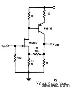
STABILIZED_BIAS
Published:2009/6/25 22:03:00 Author:May
Simple voltage-feedback loop stabilizes bias on direct-coupled FET and bipolar transistor stages. Arrangement uses constant-current source a2 to maintain stable bias voltage on base of 03. By choosing proper resistor values, DC voltage feedback from emitter of bipolar is made to control constant-cur-rent value. Any change in drain current pro-duces opposite change in constant-current value, for stabilizing bipolar. Article gives de-sign equation.-H. T. Russell, DC Feedback Stabilizes Bias on FETTBipolar Pair, EDN Magazine, Nov.15,1970, p 51. (View)
View full Circuit Diagram | Comments | Reading(1144)
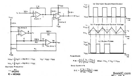
1PULSE_WIDTH_MODULATOR
Published:2009/6/25 22:02:00 Author:May
View full Circuit Diagram | Comments | Reading(736)
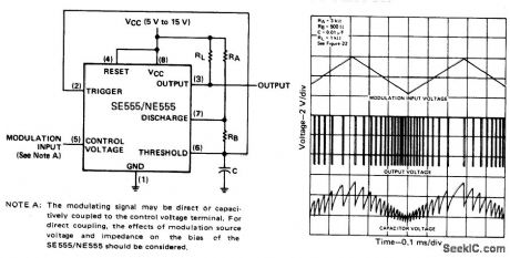
PULSE_WIDTH_MODULATOR
Published:2009/6/25 22:00:00 Author:May
If the timer is triggered with a continuous pulse train in the monostabie mode of operation, the charge time of the capacitor can be varied by changing the control voltage at pin 3.In this manner, the output pulse width can be modulated by applying a modulating signal that controls the threshold voltage. (View)
View full Circuit Diagram | Comments | Reading(0)
TELEPHONE_STATUS_MONITOR_USING_AN_oPTOISOLATOR
Published:2009/6/25 22:00:00 Author:May
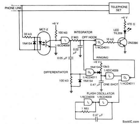
The LED indicates the status of a remote telephone. The light is off if the phone is hung up. It shines steadily if the phone is off hook, and it flashes on and off while phone rings and for 5 seconds after ringing stops. The flashing oscillator operates continuously but can drive the LED only when a ringing signal discharges the one shot capacitor to enable NAND gate G3. Thus, one oscillator handles several phone lines. (View)
View full Circuit Diagram | Comments | Reading(822)
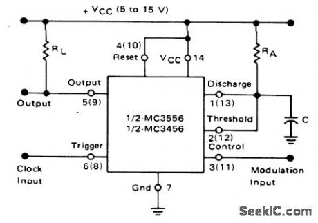
PULSE_POSITION_MODULATOR
Published:2009/6/25 21:58:00 Author:May
The threshold voltage, and thereby the time delay, of a free-running oscillator is shown modulated with a triangular-wave modulation signal; however, any modulating wave-shape could be used. (View)
View full Circuit Diagram | Comments | Reading(2)
1TV_MODULATOR
Published:2009/6/25 21:56:00 Author:May
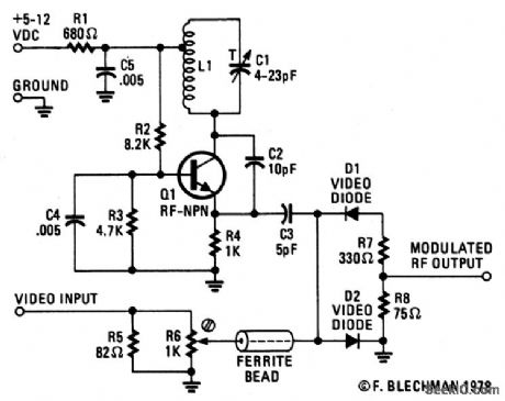
The VHF frequency is generated by a tuned Hartley oscillator circuit. Resistors R2, R3, and R4 bias the transistor, with tapped inductor L1 and trimmercapacitor C1 forming the tank circuit. Adjusting C1 determines the frequdncy. Capacitor C2 provides positive feedback from the tank circuit to the emitter at Q1. Capacitor C4 provides an RF ground for the base of Q1. Bypass capacitor C5 and resistor R1 filter out the radio frequencies generated in the tank circuit to prevent radiation from the power-supply lines. The video signal enters the parallel combination of resistors R5 and R6; this combination closely matches the 75 ohm impedance of most video cables. Resistor R6 is a small screwdrtver-adjusted potentiometer that is used to control the video input level to mixer diodes D1 and D2. (View)
View full Circuit Diagram | Comments | Reading(1302)
STEREO_BALANCER
Published:2009/6/25 21:46:00 Author:May
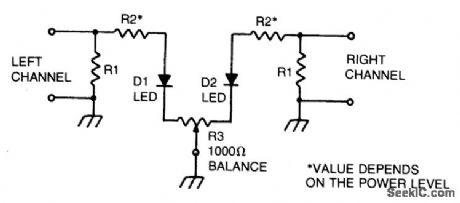
This circuit will allow you to set the gain of two stereo channels to the same level. The signal across the two channel-load resistors is sampled by resistors R2. (Values of these re-sistors will depend upon the power leveL) For most 20 milliampere LED, use approximately 2.5 K per watt. (For a 10-watt system use a 25,000 ohm resistor.) To set up, short the two inputs and connect them to one channel of a power amplifier. Apply a signal and adjust R3 until both LEDs glow at the same brightness level. The balancer is ready for use. Connect the inputs of the stereo balancer across the output of the power amplifier, and then turn up either the independent volume controls, or the balance control until both LEDs glow at the same level. To use this circuit in-line with loudspeakers, disconnect both R1s, and use the speakers as the load. (View)
View full Circuit Diagram | Comments | Reading(849)
DOUBLY_BALANCEDMIXER(BROADBAND_INPUTS,90_MHz_TUNED_OUTPUT)
Published:2009/6/25 21:33:00 Author:May

View full Circuit Diagram | Comments | Reading(578)
20_dB_VIDEO
Published:2009/6/25 21:33:00 Author:May

Simple circuit having gain of 20 dB provides 3-dB bandwidth of 20 MHz for CA3100 bipolar MOS opamp. Total noise referred to input is only 35μV RMS.- Circuit Ideas for RCA Linear ICs, RCA Solid State Di-vision, Somerville, NJ, 1977, p 12. (View)
View full Circuit Diagram | Comments | Reading(612)
ADJUSTABLE_TTL_CLOCK(MAINTAINS_50%DUTY_CYCLE)
Published:2009/6/25 21:25:00 Author:May

Symmetry of the square-wave output is maintained by connecting the right side of R2 through resistor R3 to the output of the third amplifier stage. This changes the charging cur-rent to the capacitors in proportion to the set-ting of frequency-adjusting potentiometer R2. Thus, a duty cycle of 50% is constant over the entire range of oscillation. The lower frequency limit is set by capacitor C2. With the components shown, the frequency of oscilla-tion can be varied by R2 from about 4 to 20 hertz. Other frequency ranges can be obtained by changing the values of C1 and R3, which control the upper limit of oscillation, or C2, which limits the low-frequency end. (View)
View full Circuit Diagram | Comments | Reading(782)
INVERSE_SCALER
Published:2009/6/25 21:25:00 Author:May
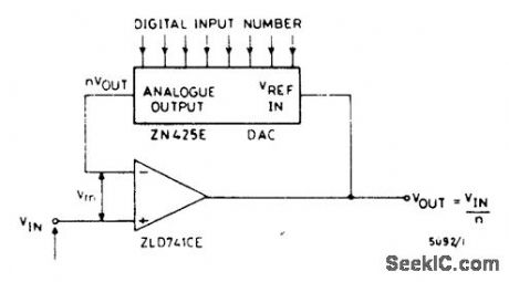
If a DAC is operated in the feedback loop of an operational amplifier,then the amplifiergain is inversely proportional to the input digital number or code to the DAC,The version giving scaling inversely proportional to posltive voltage is shown. (View)
View full Circuit Diagram | Comments | Reading(690)
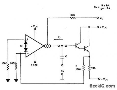
VOLTAGE_CONTROL_RESISTOR
Published:2009/6/25 21:24:00 Author:May
View full Circuit Diagram | Comments | Reading(711)
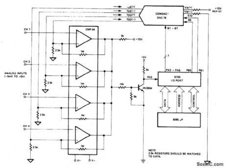
FOUR_CHANNEL_DATA_ACQUlSITION_SYSTEM
Published:2009/6/25 21:20:00 Author:May
View full Circuit Diagram | Comments | Reading(0)
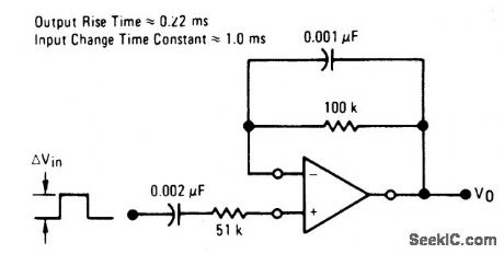
POSITIVE_EDGE_DIFFERENTIATOR
Published:2009/6/25 21:19:00 Author:May
View full Circuit Diagram | Comments | Reading(0)
STYLUS_ORGAN
Published:2009/6/25 21:18:00 Author:May
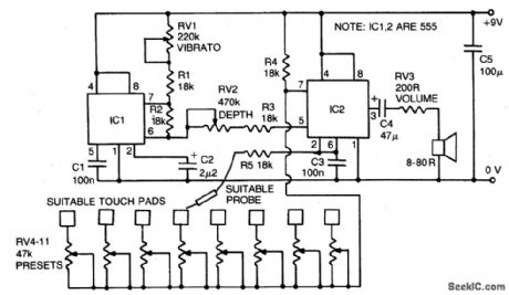
IC2 is an audio frequency oscillator. Its frequency is primarily controlled by the resistance between pins 2 and 7. RV4-11 control the oscillator frequency and by touching a stylus (connected via limiting resistor R5 to pin 2) to each preset, different notes can be played. IC1 is a low frequency oscillator (approximately 3-10Hz), the frequency of which is variable by RV1. The output of this oscillator is connected through depth control RV2 and limiting resistor R3 to the voltage control input of the audio frequency oscillator. Thus a vibrato effect occurs. (View)
View full Circuit Diagram | Comments | Reading(800)
NEGATIVE_EDGE_DIFFERENTIATOR
Published:2009/6/25 21:16:00 Author:May

View full Circuit Diagram | Comments | Reading(0)
LONG_DURATION_TIME_DELAY
Published:2009/6/25 21:14:00 Author:May
View full Circuit Diagram | Comments | Reading(0)
WIDEBAND_VARIABLE_GAIN
Published:2009/6/25 21:14:00 Author:May
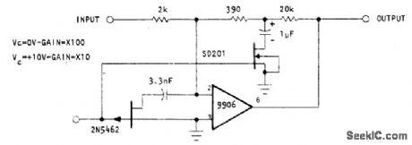
FET selves as ourPur gain-controlled device in feedback loop of Optical Electronics 9906 opamp. Resistive T network has SD201 MOS transistor as ground leg, with resistor values dlosen so transistor is electrically dose to summing junction, automatically limiting total signal voltage. Resulting arrangement of voltage-controlled feedback and compensation gives variable-gain amplifier whh good linearity and constant wideband width for all gain Ievels.- Wideband Variable Gain Amplifier, Optical Electronics, Tucson, AZ, Application Tip 10277. (View)
View full Circuit Diagram | Comments | Reading(0)
SIREN_SPACE_WAR_PHASQR_GUN
Published:2009/6/25 21:13:00 Author:May
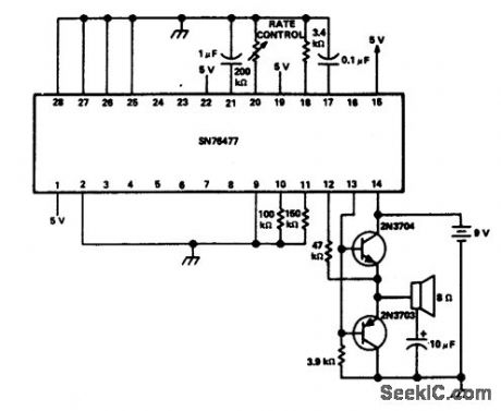
The one shot and decay functions could be added to make an ideal phasor gun sound. (View)
View full Circuit Diagram | Comments | Reading(1143)
| Pages:9/19 12345678910111213141516171819 |
Circuit Categories
power supply circuit
Amplifier Circuit
Basic Circuit
LED and Light Circuit
Sensor Circuit
Signal Processing
Electrical Equipment Circuit
Control Circuit
Remote Control Circuit
A/D-D/A Converter Circuit
Audio Circuit
Measuring and Test Circuit
Communication Circuit
Computer-Related Circuit
555 Circuit
Automotive Circuit
Repairing Circuit