
Digital Circuit
Index 10
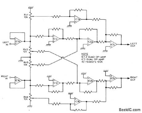
STEREO_REVERB_ENHANCEMENT_SYSTEM
Published:2009/6/25 21:12:00 Author:May
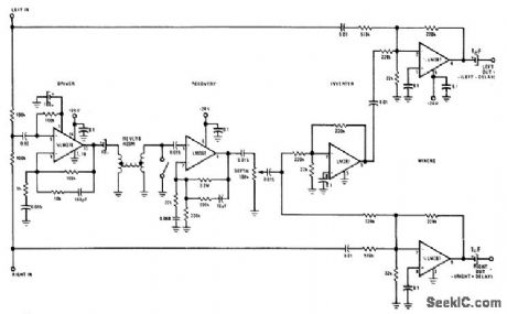
The system can be used to synthesize a stereo effect from a monaural source such as AM radio or FM-mono broadcast, or it can be added to an existing stereo (or quad) system where it produces an exciting opening up special effect that is truly impressive. (View)
View full Circuit Diagram | Comments | Reading(1133)
PROGRAMMABLE_BIRD_SOUNDS
Published:2009/6/25 21:11:00 Author:May
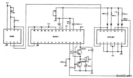
View full Circuit Diagram | Comments | Reading(696)
CAPACITANCE_MULTIPLIER
Published:2009/6/25 21:09:00 Author:May
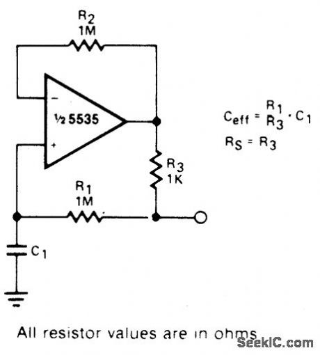
This circuit can be used to simulate large capacitances using small value components. With the values shown and C = 10 μF, an effective capacitance of 10,000 μF was obtained. The Q available is limited by the effective series resistance. So R1 should be as large as practical (View)
View full Circuit Diagram | Comments | Reading(0)
DOOR_CHIMES_DELAY
Published:2009/6/25 21:06:00 Author:May
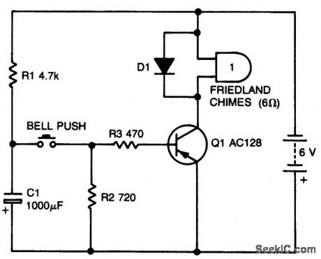
Circuit NotesWith values shown, this simple circuit will permit one operation every 10 seconds or so.Capacitor C1 charges through RI when the button is released. Making RI larger crease the delay. (View)
View full Circuit Diagram | Comments | Reading(0)
FOUR_CHANNEL_SYNTHESIZER
Published:2009/6/25 21:05:00 Author:May
This circuit will synthesize two rear chan-nels for quadraphonic sound when fed with a stereo signal. The rear output for the left chan-nel, is a combination of the left channel input 180 out of phase, added to a proportion of the right hand channel (also out of phase). The right hand rear output is obtained in a similar way. (View)
View full Circuit Diagram | Comments | Reading(0)
MICROMETRONOME
Published:2009/6/25 21:04:00 Author:May
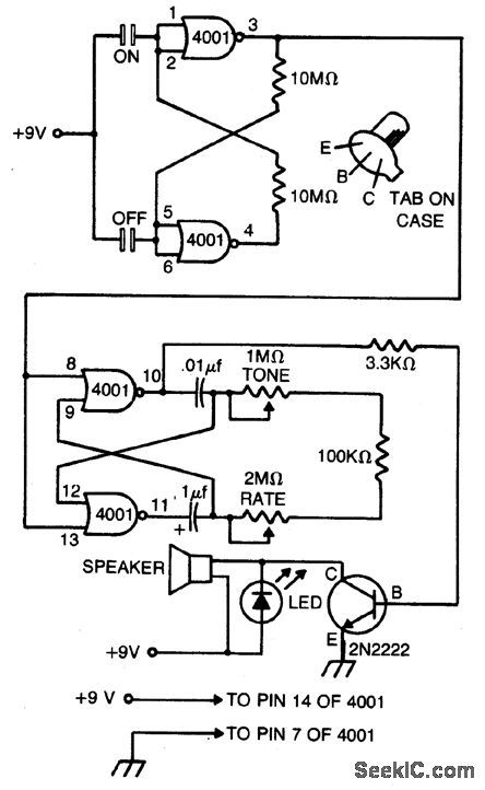
This compact metronome will run for years on a single nine-volt transistor battery.Has both tone and pulse rate controls, and uses touch plates to start and stop, can be built in a case no larger than a pack of cigarettes. The touch plates consist of two strips of metal about 1/16-inch apart mounted on, but insulated from, the case. Bridging the gap closes the switch. (View)
View full Circuit Diagram | Comments | Reading(0)
STEREO_REVERB_SYSTEM
Published:2009/6/25 21:04:00 Author:May
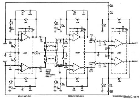
The LM378 dual power amplifier is used as the spring driver. The recovery amplifier is a low noise dual preamplifier. Mixing of the delayed signal with the original is done with another LM387 used in an inverting summing configuration. (View)
View full Circuit Diagram | Comments | Reading(0)
LONG_TIME_DELAY
Published:2009/6/25 21:02:00 Author:May
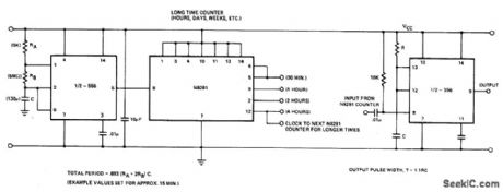
Circuit NotesIn the 556 timer, the timing is a function of the charging rate of the external capacitor. For long time delays, expensive capacitors with extremely low leakage are required. The prac-ticality of the components involved limits the time between pulses to something in the neighborhood of 10 minutes. To achieve longer time periods, both halves of a dual timer may be connected in tandem with a Divide-by ' net-work in between the first timer section oper-ates in an oscillatory mode with a period of 1/fo. This signal is then applied to a Divide-by-N network to give an output with the period of N/fo. This can then be used to trigger the second half of the 556. The total time delay is now a function of N and fo. (View)
View full Circuit Diagram | Comments | Reading(0)
MUSIC_SYNTHESIZER
Published:2009/6/25 20:57:00 Author:May
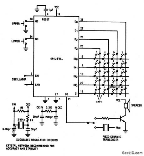
View full Circuit Diagram | Comments | Reading(800)
FET_CURVE_TRACER
Published:2009/6/25 20:34:00 Author:May
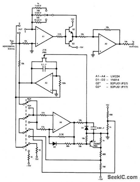
The circuit displays drain current versus gate voltage for both P and N-channel JFETS at a constant drain voltge. (View)
View full Circuit Diagram | Comments | Reading(958)
GEIGER_COUNTER
Published:2009/6/25 5:13:00 Author:May
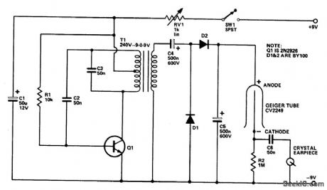
The Geiger tube needs a high voltage sup-ply which consists of Q1 and its associated components. The transformer is connected in reverse; the secondary is connected as a Hartley oscillator, and RI provides base bias.Dl, D2, C4, and C5 comprise avoltage doubler.RV1 should be set so that each click heard is nice and clean because over a certain voltage range all that will be heard is a continuous buzz. (View)
View full Circuit Diagram | Comments | Reading(0)
SENSITIVE_GEIGER_COUNTER
Published:2009/6/25 5:11:00 Author:May
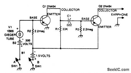
View full Circuit Diagram | Comments | Reading(648)
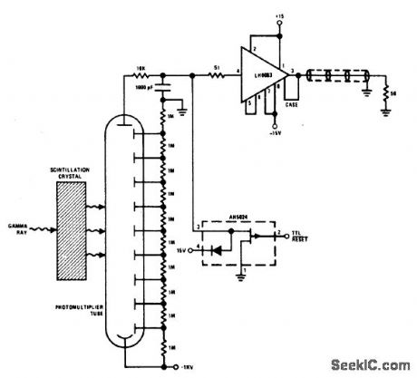
GAMMA_RAY_PULSE_INTEGRATOR
Published:2009/6/25 5:10:00 Author:May
View full Circuit Diagram | Comments | Reading(718)
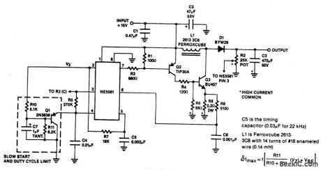
DC_TO_DC_SMPS_USING_NE5561_VARIABLE_18_V_to_30_V_OUT_AT_O2_A
Published:2009/6/25 4:32:00 Author:May
View full Circuit Diagram | Comments | Reading(621)
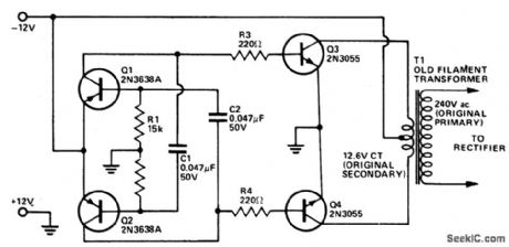
DC_TO_DC_AC_INVERTER
Published:2009/6/25 4:28:00 Author:May
Circuit Notes
This inverter uses no special components such as the torodial transformer used in many inverters. Cost is kept ldw with the use of cheap, readily available components. Essen-tially, it is a power amplifier driven by an asta-ble multivibrator. The frequency is around 1200 Hz which most 50/60 Hz power transfor-mers handle well without too much loss. In-creasing the value of capacitors C1 and C2 will lower the frequency if any trouble is experi-enced. However, rectifier filtering capacitors required are considerably smaller at the higher operating frequency. The two 2N3055 transis-tor should be mounted on an adequately sized heatsink. The transformer should be rated ac-cording to the amount of output power required allowing for conversion efficiency of approxi-mately 60%. (View)
View full Circuit Diagram | Comments | Reading(2567)
AUDIO_RF_SIGNAL_TRACER_PROBE
Published:2009/6/25 4:24:00 Author:May
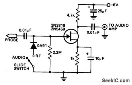
This economical signal tracer is useful for servicing and alignment work in receivers and low power transmitters. When switched to RF, the modulation on any signal is detected by the diode and amplified by the FET. A twin-core shielded lead can be used to connect the probe to an amplifier and to feed 6 volts to it. (View)
View full Circuit Diagram | Comments | Reading(3174)
PRECISION_CURRENT_SINK
Published:2009/6/25 4:18:00 Author:May
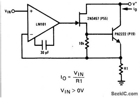
Circuit Notes
The 2N5457 JFET and PN2222 bipolar have inherently high output impedance. Using R1 as a current sensing resistor to provide feedback to the LM101 op amp provides a large amount of loop gain for negative feedback to enhance the true current sink nature of this circuit. For small current values, the 10 K re-sistor and PN2222 may be eliminated if the source of the JFET is connected to R1. (View)
View full Circuit Diagram | Comments | Reading(0)
SIMPLE_LOGIC_PROBE
Published:2009/6/25 4:17:00 Author:May
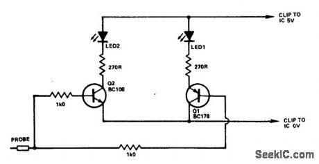
If the probe is connected to logic 0, Q1 will be turned on lighting D1. At logic 1, Q2 will be turned on lighting D2. For Q1 and Q2 any NPN or PNP transistors will do.Similarly, D1 and D2 can be any LEDs. (View)
View full Circuit Diagram | Comments | Reading(1367)
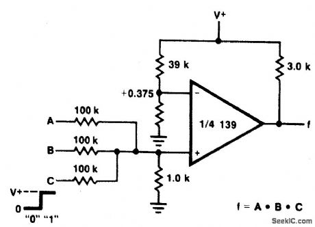
1AND_GATE
Published:2009/6/25 3:18:00 Author:May
View full Circuit Diagram | Comments | Reading(655)
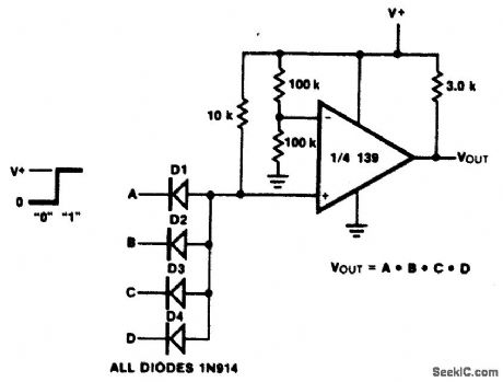
LARGE_FAN_IN_AND_GATE
Published:2009/6/25 3:18:00 Author:May
View full Circuit Diagram | Comments | Reading(778)
| Pages:10/19 12345678910111213141516171819 |
Circuit Categories
power supply circuit
Amplifier Circuit
Basic Circuit
LED and Light Circuit
Sensor Circuit
Signal Processing
Electrical Equipment Circuit
Control Circuit
Remote Control Circuit
A/D-D/A Converter Circuit
Audio Circuit
Measuring and Test Circuit
Communication Circuit
Computer-Related Circuit
555 Circuit
Automotive Circuit
Repairing Circuit