
Digital Circuit
Index 12
CURRENT_TO_VOLTAGE_CONVERTER
Published:2009/6/25 2:12:00 Author:May
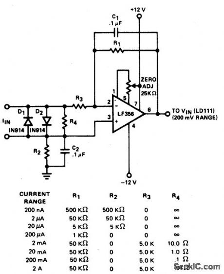
Converter features eight decades of cur-rent range. The circuit is intended to be used with the 200.0 mV range of a DVM. (View)
View full Circuit Diagram | Comments | Reading(0)
RESISTANCE_TO_VOLTAGE_CONVERTER
Published:2009/6/25 2:08:00 Author:May
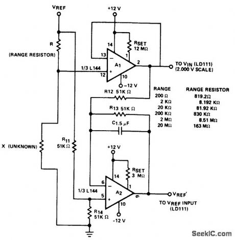
Circuit will measure accurateiy to 20 M when associated with a buffer amplifier (A1) having a low input bias current (IIN) < 30 nA). The circuit uses two of the three amplifiers contained in the Siliconix L144 micropower triple op amp. (View)
View full Circuit Diagram | Comments | Reading(1579)
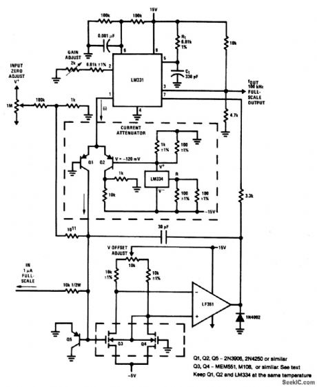
PICOAMPERE_TO_FREQUENCY_CONVERTERS
Published:2009/6/25 2:03:00 Author:May
View full Circuit Diagram | Comments | Reading(633)
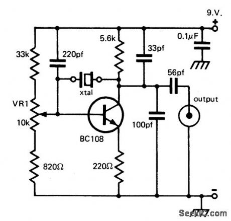
100_kHz_CRYSTAL_CALIBRATOR
Published:2009/6/25 Author:May

Circuit Notes
This circuit is often used by amateur radio operations, shortwave listeners, and other operators of shortwave receivers to calibrate the dial pointer. The oscillator operates at a fundamental frequency of 100 kHz, and the harmonics are used to locate points on the shortwave dial, provided that the output of the calibrator is coupled to the antenna circuit of the receiver. The crystal shunts the feedback voltage divider, and is in series with a variable capacitor (C3) that is used to set the actual operating frequency of the calibrator. (View)
View full Circuit Diagram | Comments | Reading(1)
MULTIPURPOSE_MODULE
Published:2009/6/24 23:41:00 Author:May

Flexible circuit using FET to drive bipolar transistor has -3 dB points at 100 Hz and 0.6 MHz. Components are noncritical and can be changed considerably in value to optimize gain, frequency response, power output, or power consumption. Load presented to FET is primarily input resistance of bipolar transistor, about 1000 ohms, which gives voltage gain of 4 for FET.-I. M Gottlieb, A New Look at Solid-State Amplifiers, Ham Radio, Feb. 1976, p 16-19. (View)
View full Circuit Diagram | Comments | Reading(0)
SUMMING_SCALING_VIDEO
Published:2009/6/24 23:31:00 Author:May

With Motorola MC1552G video amplifier connected as shown, summation of input signal currents is accom-plished at pin 4 through input resistors whose values arechosen to give desired scale factor.- A Wide Band Monolithic Video Amplifier, Mo-torola, Phoenix, AZ, 1973, AN-404, p 9. (View)
View full Circuit Diagram | Comments | Reading(652)
SINGLE_TRANSISTOR_CARRIER_CURRENT_RECEIVERTO_LINE_COUPLER
Published:2009/6/24 23:30:00 Author:May
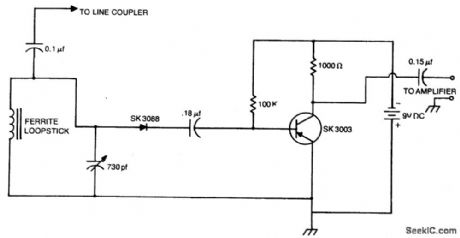
View full Circuit Diagram | Comments | Reading(645)
PHOTO_STROBE_SLAVE_TRIGGER
Published:2009/6/24 23:14:00 Author:May
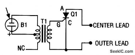
The photo strobe slave trigger circuit uses a solar cell and an SCR to flash any strobe when you trigger your master strobe. The tiny solar cell produces a vet'y small voltage when light falls on its surface. (View)
View full Circuit Diagram | Comments | Reading(0)
TOUCH_CIRCUIT
Published:2009/6/24 23:10:00 Author:May
View full Circuit Diagram | Comments | Reading(0)
PHOTO_STROBE
Published:2009/6/24 23:00:00 Author:May
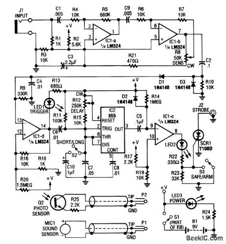
Sound or light sensors connected to J2 produce a voltage that is amplified by IC1-a and IC1-b. A positive trigger voltage that is developed by D1 and D3 and amplified by IC1-d, drives IC2 and IC1 to trigger SCR1. SCR1 is connected to a strobe. This device is handy for photographic purposes to take pictures of events that involve sound, such as impacts, etc. (View)
View full Circuit Diagram | Comments | Reading(0)
TOUCH_TRIGGERED_BISTABLE
Published:2009/6/24 22:59:00 Author:May
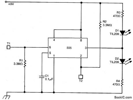
This circuit uses a 555 timer in the bista-ble mode. Touching T2 causes the output to go high; D2 conducts and Dl extinguishes. Touching T1 causes the output to go low; Dl conducts and D2 is cut off. The output from pin 3 can also be used to operate other circuits (e.g., a triac controlled lamp). In this case, the LEDs are useful for finding the touch terminals in the dark. C1 is not absolutely necessary but helps to prevent triggering from spurious pulses. (View)
View full Circuit Diagram | Comments | Reading(827)
OPTICAL_SCHMITT_TRIGGER
Published:2009/6/24 22:44:00 Author:May


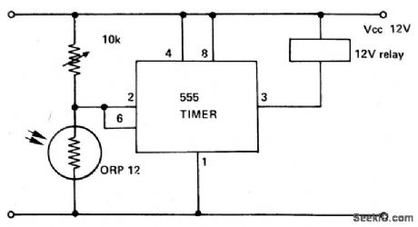
This circuit shows a 555 with its trigger and threshold inputs connected together used to energize a relay when the light level on a photoconductive cell falls below a preset value. Circuit can be used in other applications where a high input impedance and low output impedance are required with the minimum component count. (View)
View full Circuit Diagram | Comments | Reading(1206)
TIME_DELAY_FLASH_TRIGGER_CIRCUIT
Published:2009/6/24 22:43:00 Author:May

The circuit is built around a single 4093 quad 2-input NAND Schmitt trigger. Two gates from that quad package (U1-a and U1-b) are configured as a set-reset flip-flop. (View)
View full Circuit Diagram | Comments | Reading(1601)
PHASE_SHIFTER_WITH_EIGHT_OUTPUTS
Published:2009/6/24 22:39:00 Author:May
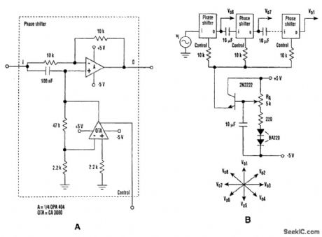
The circuit consists of eight cascaded identical cells, each cell being a dc-controlled active phase shifter. Because the dc control is common for all shifters, the circuit is adjusted by trimming RA so that the phase difference between V01 and Vi is zero. As a result, each shifter will introduce a phase difference of exactly π/r. The eight signals for PSK are available at the op amps' outputs.
Phase accuracy is acceptable for 1%-tolerance resistors and 5%-tolerance 100-nF capacitors. Also, the amplitude of Vi (which is a 1700-Hz sine wave), should not exceed 1 V. (View)
View full Circuit Diagram | Comments | Reading(925)
LONG_TAILED_PAIR_PHASE_SPLITTER
Published:2009/6/24 22:31:00 Author:May
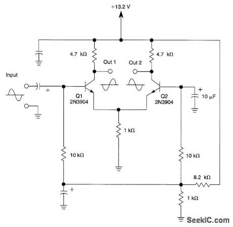
The single-phase input produces out-of-phase outputs at the collectors of Q1 and Q2. (View)
View full Circuit Diagram | Comments | Reading(914)
UNDERVOLTAGE_INDICATOR_FORBATTERY_OPERATED_EQUIPMENT
Published:2009/6/24 22:30:00 Author:May
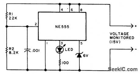
Due to the low duty cycle of flashing LED, the average current drain is 1 mA or less. The NE555 will trigger the LED on when the moni-tored voltage falls to 12 volts. The ratio of R1 to R2 only needs to be changed if it is desired to change the voltage point at which the LED is triggered. (View)
View full Circuit Diagram | Comments | Reading(763)
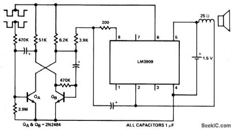
ULTRASONIC_PEST_REPELLER
Published:2009/6/24 22:28:00 Author:May
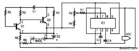
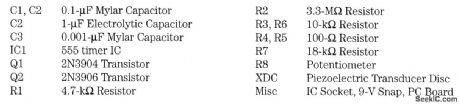
This circuit uses two transistors and one IC (555 timer IC) to produce a pulsating ultrasonic frequency. Transistors Q1 and Q2 are connected in a direct-coupled oscillator. The frequency of that oscillator is set by capacitor C1. The oscillator output is taken from the emitter of Q2 to pin 7 of IC1. Transistor Q1 is an npn transistor, and Q2 is a pnp transistor. The signal of pin 7 on IC1 causes the output signal appearing ot) pin 3 to be modulated or varied by the audio frequency developed by Q1 and Q2. The IC itself is connected as a stable multivibrator with a frequency that is determined by C3. Capacitor C3 sets the basic frequency to be well above the human hearing range (ultrasonic). The combined modulated ultrasonic frequency appears on pin 3 of IC1, where it is coupled by capacitor C4 to the piezoelectric transducer. (View)
View full Circuit Diagram | Comments | Reading(0)
GENERATE_ACCURATE_PWM_SIGNALS
Published:2009/6/24 22:21:00 Author:May
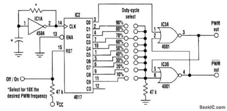
Accurate 10 to 90% duty-cycle PWM signals can be generated using this simple circuit setup.The desired duty cycle is selected by a single jumper block. PWM clock IC1 runs at 10x the desired pulse drive frequency. IC2, a 4017 divide-by-10 counter, decodes the clock pulses into one of 10 out-puts. Output 0 resets IC3, the PWM latch. The latch stays reset until the desired duty-cycle output set by the jumper block is reached. At this point, the PWM Iatch is set, and the PWM output line re-mains high until output 0 is decoded again.By calling IC2's output (0) the reset line for the latch, the PWM output is forced inactive if the jumper strap is rernoved to change duty cycles without first powering down.Using the zero-state reset allows IC2's reset pin to be used as an on/off control line for the cir-cuit. The complementary PWM output could be used in a full bridge design. (View)
View full Circuit Diagram | Comments | Reading(2110)
TRIGGER_SELECTION_CIRCUIT_FOR_OSCILLOSCOPE_TIMEBASE
Published:2009/6/24 22:17:00 Author:May
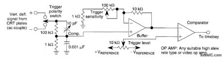
View full Circuit Diagram | Comments | Reading(782)
SIMPLE_3_DIGIT_DVM
Published:2009/6/24 22:10:00 Author:May
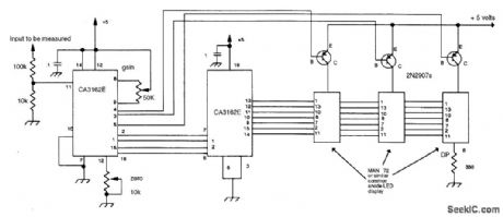
A CA3162ZE A-D converter drives a CA3161 BCD decoder/driver and LED display to form a sim-ple DVM circuit. The 50-kΩ gain control and 100-kΩ/10-kΩ voltage divider determine full-scale range. (View)
View full Circuit Diagram | Comments | Reading(1978)
| Pages:12/19 12345678910111213141516171819 |
Circuit Categories
power supply circuit
Amplifier Circuit
Basic Circuit
LED and Light Circuit
Sensor Circuit
Signal Processing
Electrical Equipment Circuit
Control Circuit
Remote Control Circuit
A/D-D/A Converter Circuit
Audio Circuit
Measuring and Test Circuit
Communication Circuit
Computer-Related Circuit
555 Circuit
Automotive Circuit
Repairing Circuit