
Digital Circuit
Index 3
74 Series digital circuit of 74LS294,74HC294 programmable divider / digital timer
Published:2011/8/1 20:44:00 Author:Lucas | Keyword: 74 Series , digital circuit , programmable divider , digital timer
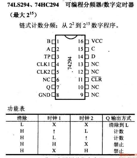
View full Circuit Diagram | Comments | Reading(1169)
74 Series digital circuit of 74LS292,74HC292 programmable divider / digital timer
Published:2011/8/1 20:45:00 Author:Lucas | Keyword: 74 Series , digital circuit , programmable divider , digital timer
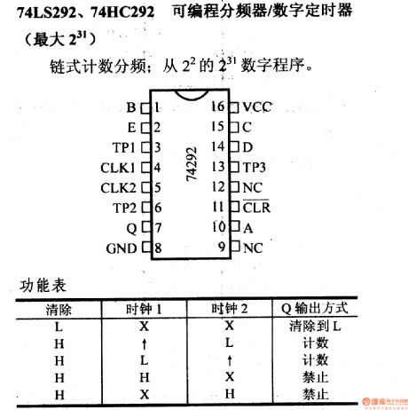
View full Circuit Diagram | Comments | Reading(1082)
74 Series digital circuit of 74285 4 × 4-bit parallel binary multiplier(low topological product)
Published:2011/8/1 20:24:00 Author:Lucas | Keyword: 74 Series , digital circuit , 4 × 4-bit parallel , binary multiplier, low topological product
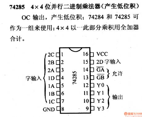
OC output can generate low topological product; 74284 and 74285 can be used in a group. 4 × 4-this part of the product is combined with a full adder.
(View)
View full Circuit Diagram | Comments | Reading(2279)
74 Series digital circuit of 74284 4 × 4-bit parallel binary multiplier(high topological product)
Published:2011/8/1 20:21:00 Author:Lucas | Keyword: 74 Series , digital circuit , 4 × 4-bit parallel , binary multiplier, high topological product
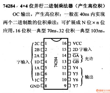
OC output can generate topological product; it typically realizes two binary numbers topological product multiplication in 40ns; it can be extended to N-bit × n-bit application, 16-bit product - typical 70ns, 32-bit product - typically 103ns.
(View)
View full Circuit Diagram | Comments | Reading(2041)
74 Series digital circuit of 74278 4-bit cascade priority register(controllable output)
Published:2011/8/1 20:46:00 Author:Lucas | Keyword: 74 Series , digital circuit , 4-bit cascade, priority register, controllable output
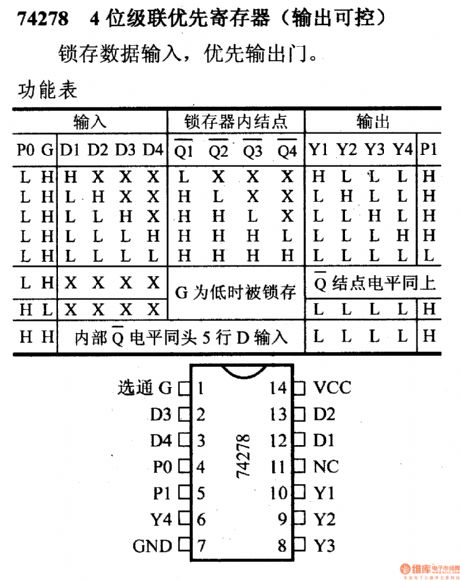
View full Circuit Diagram | Comments | Reading(810)
74 Series digital circuit of 74S274 4 × 4-bit binary multiplication (tristate)
Published:2011/8/1 23:55:00 Author:Lucas | Keyword: 74 Series , digital circuit , 4 × 4-bit , binary multiplication , tristate
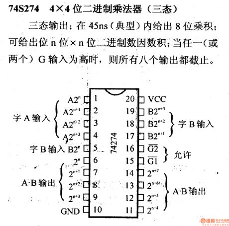
Three-state output; it has given 8-bit product in 45ns (typical); it can be given n-bit × n-bit binary numbers factor product; when any one (or two) G input is high, all eight outputs are deadline.
(View)
View full Circuit Diagram | Comments | Reading(1516)
74 Series digital circuit of 74259,74LS259 8-bit addressable latch
Published:2011/8/2 0:51:00 Author:Lucas | Keyword: 74 Series , digital circuit, 8-bit addressable latch
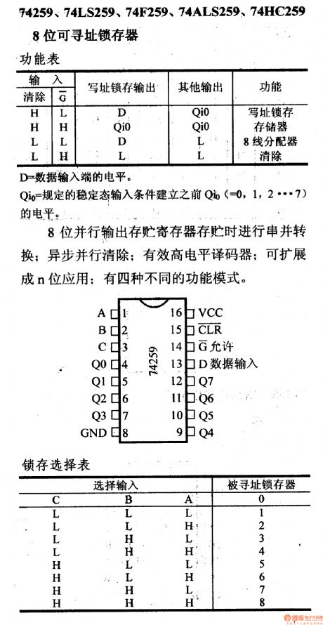
D=the level of the data input end.
Qio = the output level before establishing the steady-state input conditions.
8-bit parallel output storage register can make serial parallel conversion; asynchronous parallel clear; active high decoder; it can be extended to n-bit applications; it has four different function modes.
(View)
View full Circuit Diagram | Comments | Reading(2081)
74 Series digital circuit of 74248,74249 BCD seven segment decoder / driver
Published:2011/8/2 4:17:00 Author:Lucas | Keyword: 74 Series , digital circuit , BCD seven segment , decoder , driver

It can drive the effective high level output of light buffer; it has lamp test device; frontier, back porch are zero out; it can adjust the light intensity; 248 contains the boost resistor; 249 is the collector open circuit output, and the pin diagram is the same with 74246.
1. It requires 0 to 15, then the turning off input (BI) must remain high level, if it does not eliminate decimal zero, the dynamic turning off input (RBI) is open or high. If the low input is direct added to turning off input, all segment outputs are off regardless of the level of other inputs.
(View)
View full Circuit Diagram | Comments | Reading(2112)
74 Series digital circuit of 74246,74247 BCD seven segment decoder / driver
Published:2011/8/2 4:13:00 Author:Lucas | Keyword: 74 Series , digital circuit , BCD seven segment , decoder , driver
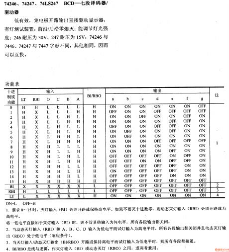
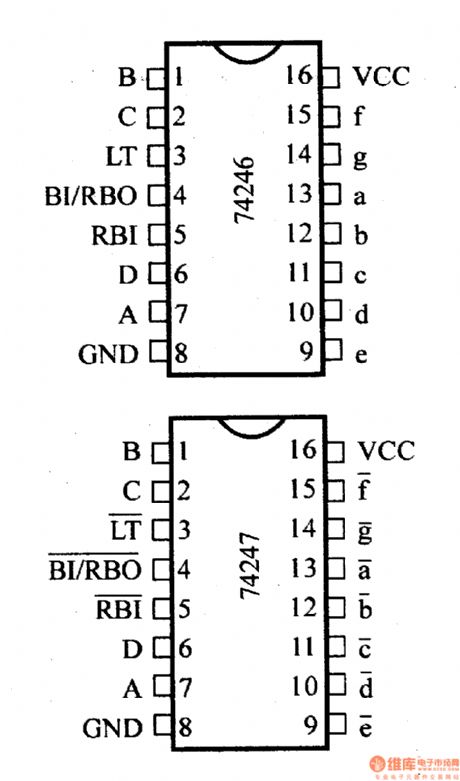
The open-collector output can directly drive the display; it has lamp test device; frontier, back porch are zero out; it can adjust the light intensity; the withstand voltage of 246 is 30V, and the withstand voltage of 247 is 15V; the 74246 and 7446,74247,7447 are similar but the word shapes, thus they are interchangeable. 1. It requires 0 to 15, then the turning off input (BI) must remain high level, if it does not eliminate decimal zero, the dynamic turning off input (RBI) is open or high. If the low input is direct added to turning off input, all segment outputs are off regardless of the level of other inputs.
(View)
View full Circuit Diagram | Comments | Reading(6296)
PROGRAMMABLE_TIMER_SEQUENCER
Published:2009/7/14 19:40:00 Author:May
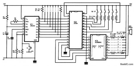
The circuit diagram of this programmable sequencer could be applied in a number of timing uses. Prior to the start of each interval, an audible tone is generated, and a seven-segment LED display shows the interval number. Prior to the end of that inerval, the buzzer sounds again. IC1 is a 2240 timer/counter device that clocks up to 256 periods, the durations of which are determined by resistor R1 and capacitor C1. The 2240 has its RESET and TRIGGER pins (10 and 11) wired via a push switch S1.The timer is used to operate a memory chip, IC2. The first 8 addressed bits are used by the timer/counter to step through the 256 steps available for each program. The other 6 bits are selected by an external switch network S2 to S7 which permits up to 26 programs, each of 256 steps. The 27C64 has eight outputs, which was enough for a single-digit LED display plus a piezo buzzer. (View)
View full Circuit Diagram | Comments | Reading(3249)
DIGITAL_LATCH_WITH_SAFETY_RESET_FEATURE
Published:2009/7/14 12:08:00 Author:May
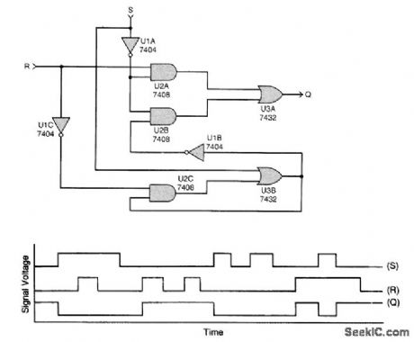
The time diagram illustrates the various modes of operation of the circuit. A high S input causes the output (Q) to go low. Thereafter, a high R input can reset Q to high, but only so long as S remains low.The asynchronous digital latching circuit is designed for use in a safety-related application, like turning off power in response to an alarm signal. During normal operation in the absence of an alarm, the SET (S) and RESET input voltages are low or off, while the output voltage (Q) is high or on. The SET input constitutes the alarm signal: Whenever S goes high (on), Q goes low (off), and thereafter remains low, even when S goes low. Thus, for example, the circuit keeps a power supply turned off even when the alarm has been shut off. If a safe condition has been restored, then the circuit can be reset to Q high by applying a high (on) signal to the RESET ( R ) input terminal. However, regardless of the R input level, Q cannot be driven high as long as S remains high; that is, the circuit cannot be reset if the alarm signal is still on. Thus, the RESET signal cannot override the alarm signal and thereby provide a false indication of safety. Also, this does not go into oscillation when the SET and RESET inputs change simultaneously.
(View)
View full Circuit Diagram | Comments | Reading(1102)
COPYING_CASSETTE_PROGRAMS
Published:2009/7/14 5:19:00 Author:May
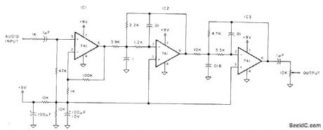
Controller serves for making duplicate copies of microprocessor programs recorded on magnetic tape, for insurance against accidental damage to master cassette during use. Used between audio out- put of cassette player and audio input of tape recorder. Opamp IC1 with gain of 100 overloads so output is constant-amplitude square wave regardless of input level from tape being copied. If program uses audio tones for digital data, eight cycles of 2400 Hz represents digital 1 and four cycles of 1200 Hz represents digital O. Additional opamps act as four-pole Butterworth filter rejecting signals above 3000 Hz. 10K pot is adjusted so output level matches requirements of recorder,-P. A. Stark, Copying Computer Cassettes, Kilobaud, Aug. 1978, p 94-96. (View)
View full Circuit Diagram | Comments | Reading(854)
DIGITALLΥ__PROGRAMMED_INPUTS_AND_GAINS
Published:2009/7/14 4:59:00 Author:May
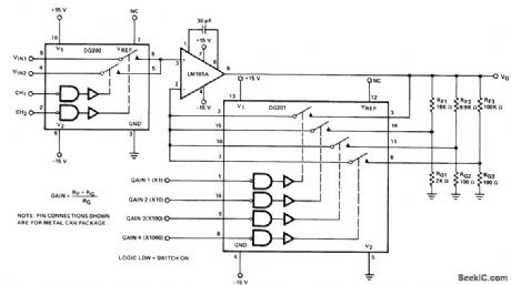
DG200 CMOS analog switch gives programmable choice of two inputs to opamp, and DG201 switch gives choice of four different gain values (1, 10, 100, or 1000) for opamp. Full opamp output range of ±12 V is provided even for unity-gain position of switch.-″Analog Switches and Their Applications,″ Siliconix, Santa Clara,CA,1976,p7-67. (View)
View full Circuit Diagram | Comments | Reading(654)
100_dB_DYNAMIC_RANGE
Published:2009/7/14 3:11:00 Author:May
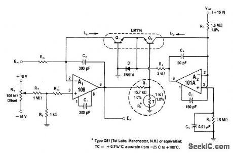
Circuit generates log ratio of currents Ic1, and Ic2, with accuracy within 3% from 10 nA to 1 mA (100dB range) when Ic2 is fixed at 10-μA reference value. Accuracy increases to 1% for current inputs between 40 nA and 400 μA (80 dB). A2 supplies constant reference current to Q2.Q1 is operated as transdiode withQ2 providing temperature compensation of offset voltage.-W. G. Jung, IC Op-Amp Cookbook, Howard W. Sams, Indianapolis, IN, 1974 ,p 213-214. (View)
View full Circuit Diagram | Comments | Reading(802)
PROGRAMMABLE_FREQUENCY_STATE_VARIABLE
Published:2009/7/14 3:03:00 Author:May
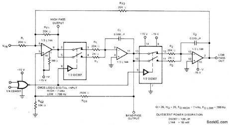
Provides choice of low-pass, high-pass, and bandpass out puts with logic-selectable center frequency of 700 or 7000 Hz. Logic input controls DG307 low-power dual analog switch for changing values of frequency-determining resistors R1 and R2.-″Analog Switches and Their Applications,″Siliconix, Santa Clara,CA,1976, p 7-86. (View)
View full Circuit Diagram | Comments | Reading(867)
DIGITALLY_SELECTABLE_GAIN
Published:2009/7/14 2:59:00 Author:May
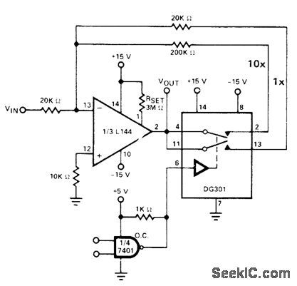
TTL controls operation of DG301 low-power analog switch at output of inverting opamp. Low logic gives gain of 1, and high logic gives gain of 10.- Analog Switches and Their Applications, Siliconix, Santa Clara, CA, 1976, p 7-90.
(View)
View full Circuit Diagram | Comments | Reading(896)
REMOTE_DIGITAL_PROGRAMMING_OF_TIMER
Published:2009/7/13 2:16:00 Author:May
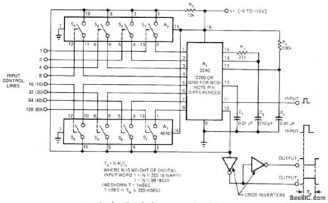
Either binary or BCD logic can be used for selecting delay interval of monostable timer A1, with delays being integral multiples of shortest time. Timing is programmed by pair of 4016 CMOS analog switches, A2 and A3. Given timing tap is activated when corresponding digital input control line is high and deactivated when control is low. Programmable timing range is 1 to 255 ms for 2240, and 1 to 99 ms for 2250 or 8250 timer. Basic interval can bechanged to suit other applications. CMOS output buffer stage ensures valid output logic Ievels. Although circuit will operate over supply range indicated, operation is optimum forsupply of 10 to 15V.-W. G. Jung, Take a Fresh Look at New IC Timer Applications, EDN Magazine, March 20, 1977, p 127-135. (View)
View full Circuit Diagram | Comments | Reading(841)
DIGITAL_COMPASS
Published:2009/7/10 4:29:00 Author:May
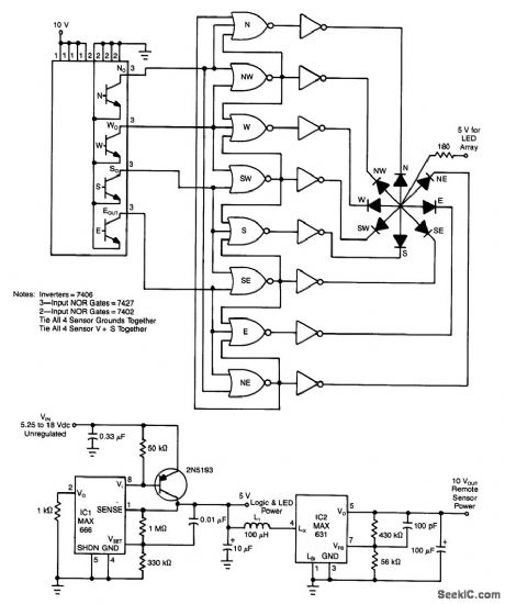
A four output Hall sensor combined with a few logic gates produce this digltal compass. The NOR gates resolve the four Hall outputs into eight distinct compass directions. LEDs to indicate direction aredriven by eight inverters. A power supply for 5.25-to 18-Vdc operation IS shown in the figure. (View)
View full Circuit Diagram | Comments | Reading(2052)
DIGITALLY_SELECTABLE_INPUTS_AND_GAIN
Published:2009/7/9 20:52:00 Author:May
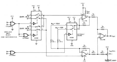
Low-power DG306 and DG305 analog switehes provide choice of 10.4 or 101 gain and choice of two differential input channels for instrumentation applications. Highest gain is obtained when control logic is high.- Analog Switches and Their Applications,''siliconix,Santa Clara,CA,1976,p 7-91. (View)
View full Circuit Diagram | Comments | Reading(876)
Digital programmable voltage reference circuit diagram with 0 ~ 9.99V Output voltage
Published:2011/5/10 4:21:00 Author:Rebekka | Keyword: Digital programmable voltage reference, 0 ~ 9.99V output voltage
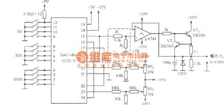
Figure shows the output voltage 0 ~ 9.99V digital programmable reference voltage source circuit. The circuit is composed of 12-bit D / A converter, DAC-80-CCD-V, VT1, VT2, the current amplifier and other components. The larger output current is, the more widespread use it will hace. But it is used for experiment and adjustment of the reference voltage source. The output current is 100mA. If the step voltage is set to be 1mV, you need to add an attenuator composed of the resistance Rl and R2. The output voltage is 0 ~ 9.99V. In Circuit, RPl is used for full-scale adjustment, RP2 is used for zero.
(View)
View full Circuit Diagram | Comments | Reading(2078)
| Pages:3/19 12345678910111213141516171819 |
Circuit Categories
power supply circuit
Amplifier Circuit
Basic Circuit
LED and Light Circuit
Sensor Circuit
Signal Processing
Electrical Equipment Circuit
Control Circuit
Remote Control Circuit
A/D-D/A Converter Circuit
Audio Circuit
Measuring and Test Circuit
Communication Circuit
Computer-Related Circuit
555 Circuit
Automotive Circuit
Repairing Circuit