
Digital Circuit
Index 13
TWISTED_PAIR_VIDEO_DRIVER_RECEIVER_CIRCUIT
Published:2009/6/24 21:51:00 Author:May
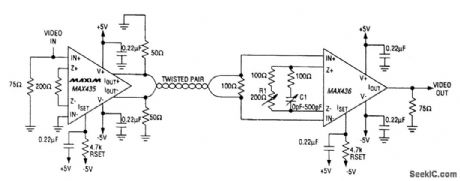
This circuit should be useful where a twisted-pair video line is to be used. R1 is adjusted for proper gain (monitor brightness and contrast) and C1 is adjusted for best color. (View)
View full Circuit Diagram | Comments | Reading(1321)
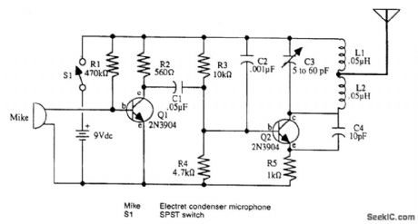
FM_BUG
Published:2009/6/24 21:24:00 Author:May
View full Circuit Diagram | Comments | Reading(752)
SIGNAL_TRACER
Published:2009/6/24 21:13:00 Author:May
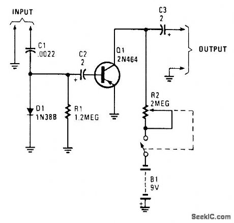
This circuit uses a simple detector-audio am-plifier. The output can be connected to head-phones or another audio amplifier. (View)
View full Circuit Diagram | Comments | Reading(0)
CABLE_TRACER
Published:2009/6/24 21:12:00 Author:May
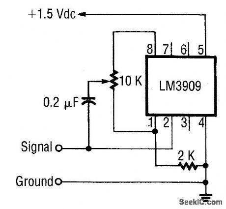
This circuit generates a 1-kHz square wave for cable tracing. Because this circuit is simple and generates from 1.5 V, several can be used at the same time to generate multiple tones for tracing multiconductor cables. (View)
View full Circuit Diagram | Comments | Reading(0)
LOW_DRIFT_SAMPLE_AND_HOLD
Published:2009/6/24 20:59:00 Author:May
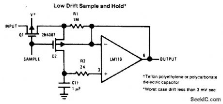
View full Circuit Diagram | Comments | Reading(0)
CRYSTAL_CHECKER
Published:2009/6/24 20:59:00 Author:May
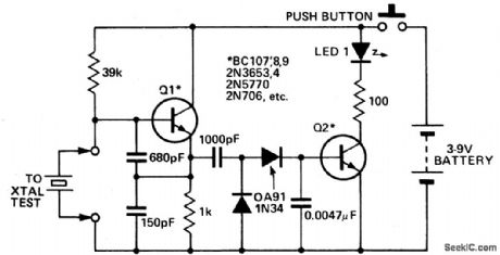
Use this circuit for checking fundamental HF crystals on a 'Go-No-Go' basis. An untuned Colpitts oscillator drives a voltage multiplier rectifier and a current amplifier. If the crystal oscillates, Q2 conducts and the LED lights. A3 or 6V, 40mA bulb could be substituted for the LED. (View)
View full Circuit Diagram | Comments | Reading(0)
ASYMMETRICAL_THIRD_ORDER_BUTTERWORTH_ACTIVE_CROSSOVER_NETWORK
Published:2009/6/24 20:38:00 Author:May
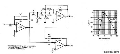
View full Circuit Diagram | Comments | Reading(0)
ABSOLUTE_TEMPERATURE_LOG_WITH_RS_232
Published:2009/6/24 4:08:00 Author:May
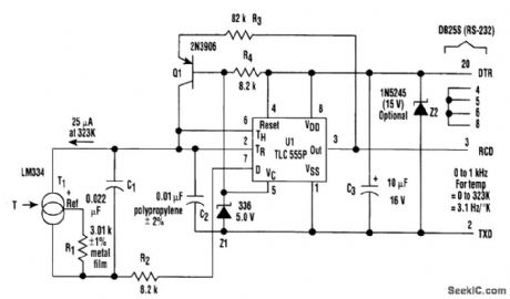
In the setup, T1 (an LM334 temperature sensor) generates a constant current that's propor-tional to absolute temperature, and equal to 25μA at 323 Kelvin (50℃). RI sets this constant of pro-portionality. The current discharges the parallel combination of C1 and C2 connected to the trigger and the threshold pins of UI, which is a CMOS implementation of the venerable 555 analog timer.The negative-going ramp is compared by UI to an internal2.S-V trigger level controlled by 21. When the ramp gets there, U1 triggers. The output pin (3) will go high, presenting a start bit to the con-nected communications port, which causes Q1 to source 100 μA to the timing node. At the same time, the discharge pin (7) will open, allowing R2 and the bottom end of C1 and T1 to be supplied by C1, and isolates it from C2.
Consequently, the current supplied by transistor Q1 will go solely to C2 so that when the result-ing positive-going ramp reaches 5V, exactly 25nC (2.5 V x C2) will have been deposited in the tim-ing node by the recharge cycle because its threshold level (6) will have been reached. This causes both the output pin to return to the negative rail, restoring the marking condition of the R2-232 in-terface, and Q1 to stop recharging C2. U1's discharge pin (7) now connects R2 to the negative rail, causing the charge that was deposited by T1 on C1 during the recharge interval to rapidly redistrib-ute between C1 and C2. This arrangement creates a very linear (0.01%) relationship between T1 cur-rent and pulse output frequency.
While this is happening, the PC's communications port hardware assembles a valid (although meaningless) character because the positive pulse output by UI looks like the start bit of a charac-ter. A simple program running in the PC can then count the frequency of these characters and con-vert the resulting rate into a direct readout of temperature. Because of the 3.1-Hz/degree slope of frequency versus temperature, a 30-second average suffices for 0.01°resolution. (View)
View full Circuit Diagram | Comments | Reading(0)
PLD_SYNCHRONIZES_ASYNCHRONOUS_INPUTS
Published:2009/6/24 3:26:00 Author:May
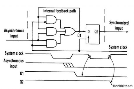
A programmable electrically erasable logic (PEEL) device can easily supply the synchronizing function. Digital systems often require synchronization of asynchronous inputs to avoid the potential metastability problems caused by setup-time violations. A common synchronization method uses two rippled 74LS72 D-type flip-flops.In this circuit, the asynchronous input feeds into the D input of the first flip-flop and its Q out-put feeds into the D of the second. Because the first flip-flop latches on the falling edge of the sys-tem clock, to avoid setup-time violations, the D input signal to the second flip-flop will be stabilized before the rising edge of the clock. Even experienced programmable-logic device designers often re-sort to such a TTL flip-flop circuit to handle the synchronization function, because of the architec-tural limitations of standard PLDs.A programmable elect;ically erasable logic (PEEL) device, such as the PEEL18CV8 from ICT, however, can easily supply the function. The user-programmable 12-configuration I/O macrocells in the device can internally feed back a signal before the output register. With this feedback arrange-ment, designing a two-stage input is simple.A gated-latch internally latches the asynchronous input on the falling edge of the system clock, generating signal Q1. ANDing the input with Q1 through the internal feedback path, eliminates a pos-sible hazard condition during the clock's high-to-low transition time. The latch then holds Q1 stable to ensure meeting the setup-time requirement of the subsequent D flip-flop, which, as before, regis-ters the signal on the next rising system clock edge.If by chance the input pulse width violates the set-up time of the gated latch, the clock's low time will give more time for settling. (View)
View full Circuit Diagram | Comments | Reading(0)
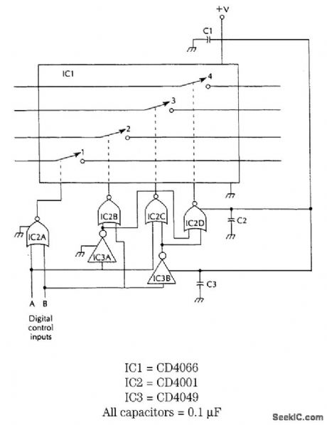
DIGITALLY_CONTROLLED_ONE_OF_FOUR_ANALOG_SWITCH
Published:2009/6/24 3:15:00 Author:May
View full Circuit Diagram | Comments | Reading(0)
125_MHz_LOGIC_PROBE
Published:2009/6/24 3:06:00 Author:May
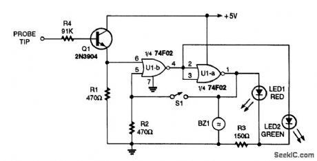
This logic probe features either high-low (LED) indication or latching operation. When S1 closed, the indication of a pulse is latched and the red LED1 stays on. Piezoelectric buzzer BZ1 used as a beeper to sound that a logic high is preset. (View)
View full Circuit Diagram | Comments | Reading(0)
SIMPLE_RF_PROBE
Published:2009/6/24 3:05:00 Author:May
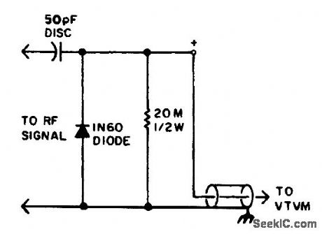
Your VTVM can measure peak voltage up to 200 MHz by using this probe. The maximum RF that can be measured is determined by the diode; with a 1N60, the probe is Iimited to 30 V. To increase the capacity, substitute a higher-voltage small-signal detector diode. House the circuit in a metal enclosure and use shielded wire. (View)
View full Circuit Diagram | Comments | Reading(1597)
MUSICAL_INSTRUMENT_DIGITAL_INTERFACE(MIDI)TRANSMITTER
Published:2009/6/24 1:54:00 Author:May
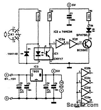
Used for digital control of musical instruments, this transmitter converts the digital data signals to equivalent optical signals for fiberoptic cable interface. Optocoupler IC1 provides isolation, and drives IC2-a and -b and T1, and finally provides a cable driver LED (SFH750). (View)
View full Circuit Diagram | Comments | Reading(1998)
CURRENT_LIMITING_REGULATOR_CIRCUIT
Published:2009/6/23 3:25:00 Author:May
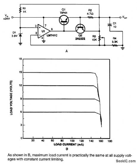

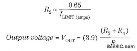
This regulator uses the drop across R2 to turn on Q2, removing base drive from Q1 and reducing the current through R1. About 0.65 V must be dropped across R2 before limiting occurs. To set limit current, (View)
View full Circuit Diagram | Comments | Reading(1246)
COMPLEMENTARY_OR_BILATERAL_ac_EMITTER_FOLLOWER_CIRCUIT
Published:2009/6/23 2:20:00 Author:May
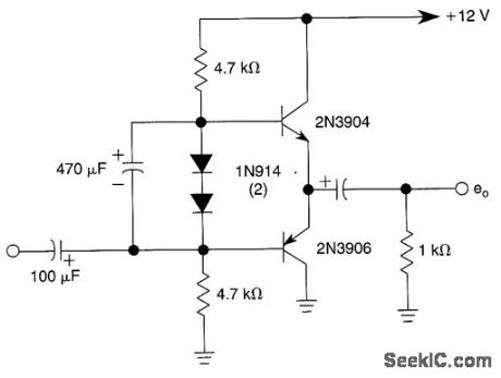
This noninverting circuit uses a pair of com-plementary npn (2N3904) and pnp (2N3906) transistors. (View)
View full Circuit Diagram | Comments | Reading(0)
PRECISION_POWER_BOOSTER
Published:2009/6/23 2:13:00 Author:May
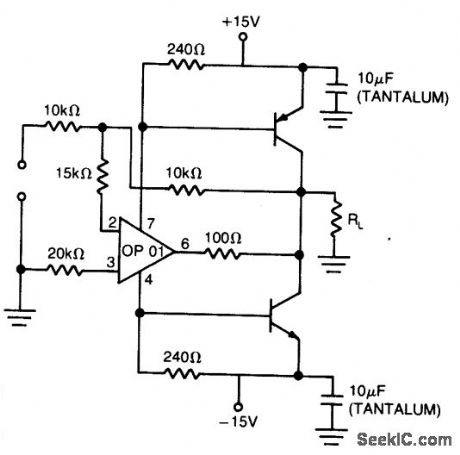
View full Circuit Diagram | Comments | Reading(766)
500_ksps_8_CHANNEL_DATA_DCQUISITION_CIRCUT
Published:2009/6/23 2:10:00 Author:May
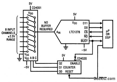
The high input impedance of the LTC1278 allows multiplexing without abuffer amplifier. Both sin-gle channel and multiplexed high-speed data acquisition systems benefit from the LTC1278/LTC1279's dynamic conversion performance. The 1.6-μs and 1.4-μs conversion and 200-ns and 180-ns S/H acquisition times enable the LTC1278/LTC1279 to convert a 500 ksps and 600 ksps, respectively. The figure shows a 500-ksps 8-channel data acquisition system. The LTC1278's high input impedance eliminates the need for a buffer amplifier between the multiplexer's output and the Adc's input. (View)
View full Circuit Diagram | Comments | Reading(0)
PRECISION_PROCESS_CONTROL_INTERFACE
Published:2009/6/23 2:03:00 Author:May
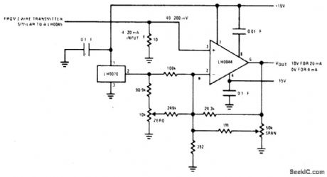
View full Circuit Diagram | Comments | Reading(0)
1_dB_PAD
Published:2009/6/23 2:03:00 Author:May

The 1-dB pad is useful as a termination in RF work to limit possible mismatch range between system blocks, etc. (View)
View full Circuit Diagram | Comments | Reading(0)
DISCRETE_CURRENT_BOOSTER
Published:2009/6/23 2:02:00 Author:May
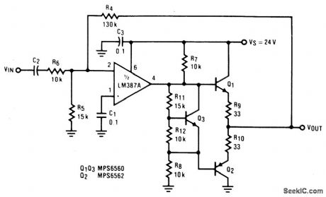
View full Circuit Diagram | Comments | Reading(0)
| Pages:13/19 12345678910111213141516171819 |
Circuit Categories
power supply circuit
Amplifier Circuit
Basic Circuit
LED and Light Circuit
Sensor Circuit
Signal Processing
Electrical Equipment Circuit
Control Circuit
Remote Control Circuit
A/D-D/A Converter Circuit
Audio Circuit
Measuring and Test Circuit
Communication Circuit
Computer-Related Circuit
555 Circuit
Automotive Circuit
Repairing Circuit