
Digital Circuit
Index 5
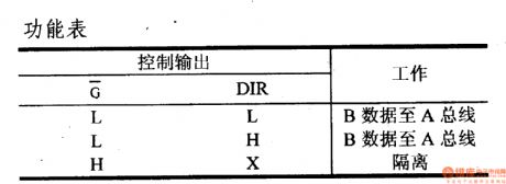
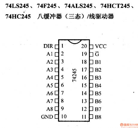
74 Series digital circuit of 74LS245,74F245 eight inverting buffer(three-state)/line driver
Published:2011/8/1 1:10:00 Author:Lucas | Keyword: 74 Series, digital circuit , eight inverting buffer, three-state), line driver
View full Circuit Diagram | Comments | Reading(4512)
74 Series digital circuit of 74290,74LS290 decimal counter
Published:2011/7/29 1:38:00 Author:Lucas | Keyword: 74 Series , digital circuit , decimal counter
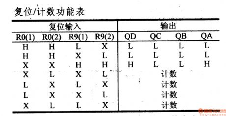
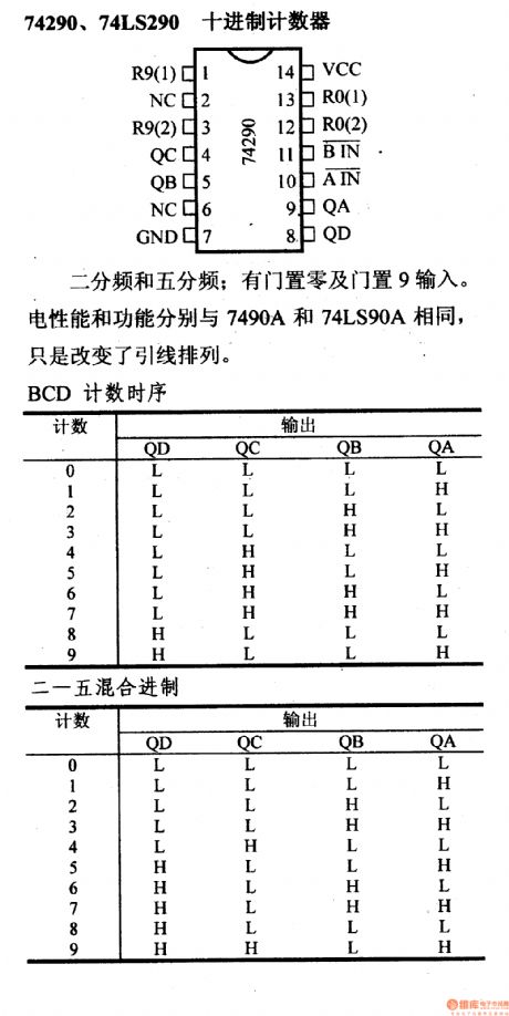
Frequency-halving and one-fifth frequency; it has zero gate and 9 inputs. Electrical performance and functionality are the same with the 7490A and 74LS90A. It just changes the lead arrangement.
(View)
View full Circuit Diagram | Comments | Reading(1830)
74 Series digital circuit of 74279,74LS279 four R-S latch
Published:2011/8/1 1:50:00 Author:Lucas | Keyword: 74 Series , digital circuit , four R-S latch
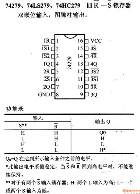
74279,74LS279, 74HC279four R-S latch
Double-clamped input, totem pole output
Q0 =the output level before establishing the steady-state input conditions.
If the output level is stable, when the S and R simultaneously reach high level, the state can not be maintained. For the latch with two S inputs; H = two L inputs, which is high; L = one or two S inputs ,which is low.
(View)
View full Circuit Diagram | Comments | Reading(3387)
74 Series digital circuit of 74276 four JK flip-flop
Published:2011/7/29 1:47:00 Author:Lucas | Keyword: 74 Series , digital circuit, four JK flip-flop
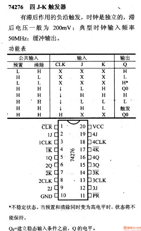
It has the negative edge trigger with lag effect, and the clock is independent, then the hysteresis is typically 200mv; typical clock input frequency is 50MHz; it has buffer output.Unsteady state. When the preset and clear goes high at the same time, the state will not be maintained.
Q0 = the output level of Q before establishing the steady-state input conditions.
(View)
View full Circuit Diagram | Comments | Reading(1561)
74 Series digital circuit of 74273,74LS273 eight D flip-flop (with clear side)
Published:2011/8/1 1:42:00 Author:Lucas | Keyword: 74 Series , digital circuit , eight D flip-flop , (with clear side
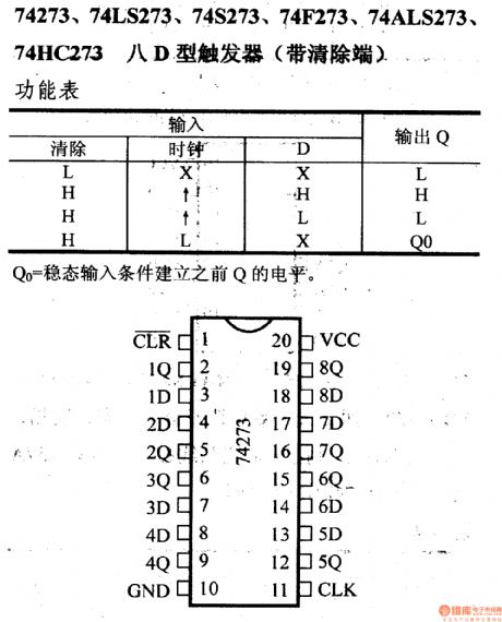
Q0 = the output level before establishing the steady-state input conditions.
(View)
View full Circuit Diagram | Comments | Reading(2887)
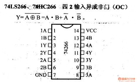
74 Series digital circuit of 74LS266,74HC266 four 2 input XNOR(OC)
Published:2011/8/1 4:25:00 Author:Lucas | Keyword: 74 Series , digital circuit , four 2 input, XNOR, OC
View full Circuit Diagram | Comments | Reading(1996)
74 Series digital circuit of 74265 four complementary output circuit
Published:2011/8/1 1:40:00 Author:Lucas | Keyword: 74 Series , digital circuit, four complementary output
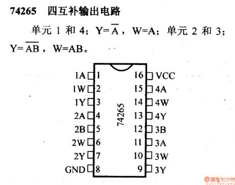
Units 1 and 4; Y=A,W=A; units 2 and 3; Y=AB, E=AB.
(View)
View full Circuit Diagram | Comments | Reading(799)
74 Series digital circuit of 74LS261 2 × 4-bit parallel binary multiplier
Published:2011/8/1 20:04:00 Author:Lucas | Keyword: 74 Series , digital circuit , 2 × 4-bit parallel , binary multiplier
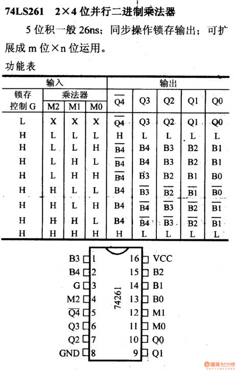
5-bit is general 26ns; synchronization latch output; it can be extended to m-bit × n-bit application.
(View)
View full Circuit Diagram | Comments | Reading(1964)
74 Series digital circuit of 74LS257A,74F257 4-bit 2-to-1 data selector(tristate,in-phase)
Published:2011/7/25 4:27:00 Author:Lucas | Keyword: 74 Series, digital circuit , 4-bit , 2-to-1 data selector, tristate, in-phase
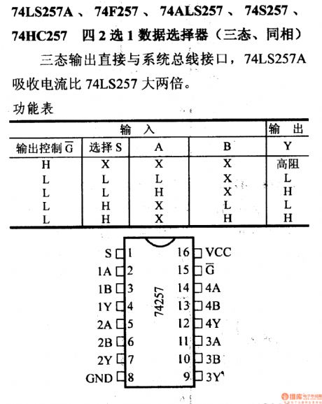
Three-state output is directly connected to the bus interface of the system, and 74LS257SA absorption current is 2 times larger than the 74LS257.
(View)
View full Circuit Diagram | Comments | Reading(1161)
74 Series digital circuit of 74LS256, 74F256 dual 4-bit addressable latch
Published:2011/8/1 4:32:00 Author:Lucas | Keyword: 74 Series , digital circuit , dual 4-bit , addressable latch
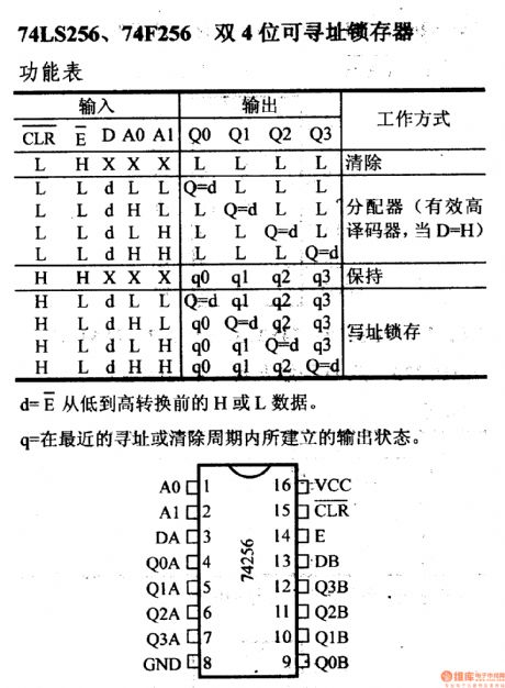
d = The H ot L data E before the conversion from low to high; q = the output state in the recent addressing or clearing cycle.
(View)
View full Circuit Diagram | Comments | Reading(833)
74 Series digital circuit of 74251,74LS251 8-to-1 data selector/driver(tristate)
Published:2011/8/1 4:23:00 Author:Lucas | Keyword: 74 Series, digital circuit , 8-to-1 data selector, driver, tristate
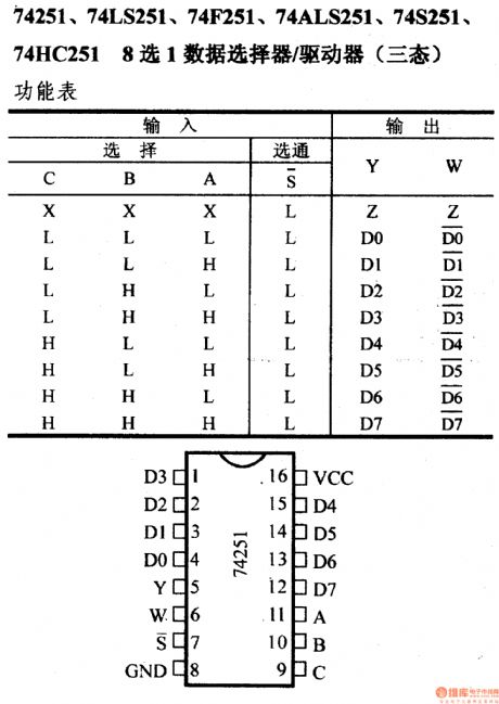
View full Circuit Diagram | Comments | Reading(1746)
74 Series digital circuit of 74LS253,74S253 dual 4 to 1 data selector (tristate)
Published:2011/8/1 1:38:00 Author:Lucas | Keyword: 74 Series , digital circuit , dual data selector, 4 to 1, tristate
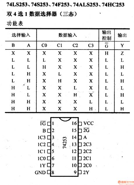
View full Circuit Diagram | Comments | Reading(936)
74 Series digital circuit of 74LS244,74F244 eight inverting buffer/line driver/ line receiver(three-state)
Published:2011/8/1 1:08:00 Author:Lucas | Keyword: 74 Series, digital circuit, eight inverting buffer, line driver, line receiver, three-state
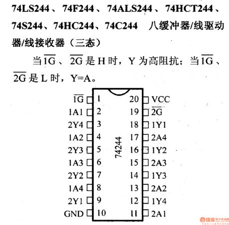
When 1G, 2G are H, Y is in high resistance; when 1G, 2G are L, Y=A.
(View)
View full Circuit Diagram | Comments | Reading(3489)
74 Series digital circuit of 74LS241,74F241 eight inverting buffer/line driver/ line receiver(three-state)
Published:2011/8/1 1:06:00 Author:Lucas | Keyword: 74 Series , digital circuit , eight inverting buffer, line driver , line receiver, three-state
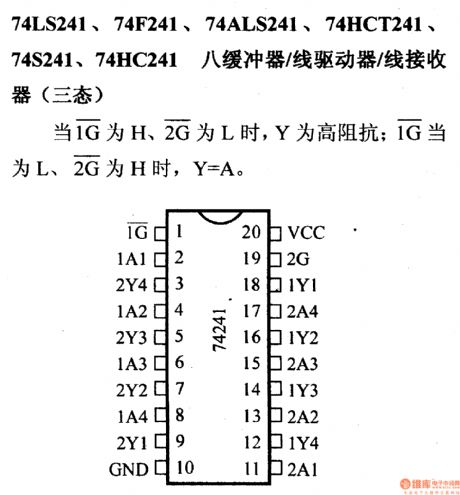
When 1G is H, 2G is L, Y is in high resistance; when 1G is L, and 2G is H, Y=A.
(View)
View full Circuit Diagram | Comments | Reading(1036)
74 Series digital circuit of 74S226 4-bit parallel latched bus transceiver
Published:2011/7/31 22:37:00 Author:Lucas | Keyword: 74 Series, digital circuit , 4-bit parallel latched, bus transceiver
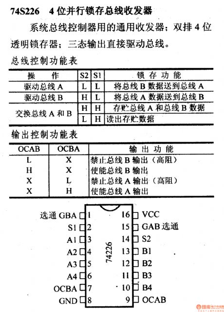
The universal transceiver for system bus controller; double 4-bit transparent latch; one state output can directly drive the bus.
(View)
View full Circuit Diagram | Comments | Reading(1110)
74 Series digital circuit of 74198 8-bit shift register
Published:2011/7/29 1:26:00 Author:Lucas | Keyword: 74 Series , digital circuit , 8-bit shift register
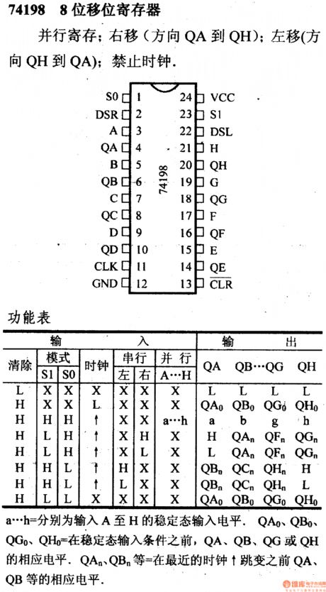
Parallel storage; right shift(direction is from the QA to QH): left shift(direction is from the QH to QA); it forbids the clock.
a. .. h= the input of steady-state input level of A to H.
QAo,QBo, QGo, QHo=the input of steady-state input level of QAo,QBo, QGo, QHo.
QAn, QBn= the corresponding level ofQA, QB before the next jump of the clock.
(View)
View full Circuit Diagram | Comments | Reading(2145)
INSTANT_VSWR_BRIDGE
Published:2009/6/28 22:01:00 Author:May

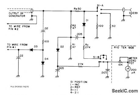
Modified 190B Tektronix constant-amplitude signal generator is combined with 50-ohm resistance bridge toglve stable high-accuracy instrument for measuring voltage standing-wave ratio as guide fortuning antennas Range iS 160 meters through 10 meters,Trim Rx so incident or forward voltage at position 1 of S1 equals reflected voltage at position 2. Article gives chart for finding VSWR. Step-by-step procedure for modifying signal generator is given.-D.Sander, Make Antenna Tuning a Joy, 73 Magazine, May 1978, p 134-136. (View)
View full Circuit Diagram | Comments | Reading(1159)
74 Series digital circuit of 74195,74LS195A 4-bit parallel access shift register
Published:2011/8/1 0:56:00 Author:Lucas | Keyword: 74 Series, digital circuit , 4-bit parallel access , shift register
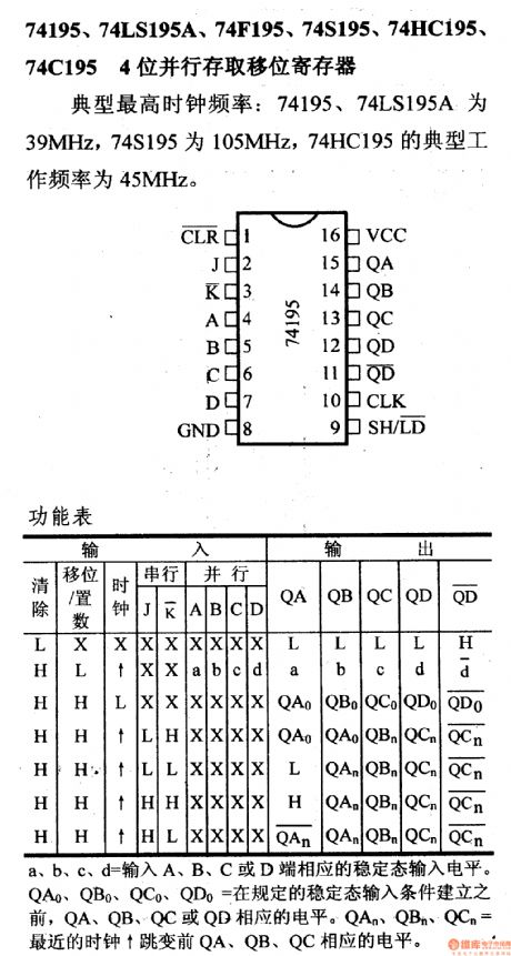
The typical maximum clock frequency of 74195,74 LS195A is 39MHz, and 74S195 is 105MHz; the typical operating frequency of 74HC195 is 45Hz.
a, b, c, d = the corresponding steady input level of A, B, C, D. QA0, QB0, QC0, QD0= the corresponding level of QA, QB, QC, QD before the establishment of steady-state input conditions. QAn, QBn, QCn= the corresponding level of QA, QB, QC at the latest time hopping.
(View)
View full Circuit Diagram | Comments | Reading(4005)
74 Series digital circuit of 74194,74LS194A 4-bit two-way general shift register
Published:2011/8/1 0:53:00 Author:Lucas | Keyword: 74 Series , digital circuit , 4-bit two-way , general shift register
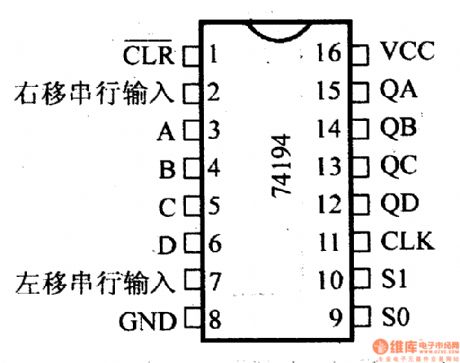
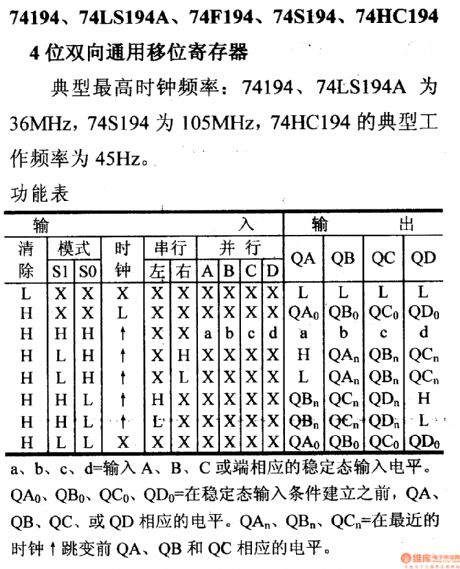
The typical maximum clock frequency of 74197,74 LS194A is 36MHz, and 74S194 is 104MHz; the typical operating frequency of 74HC194 is 45Hz.
a, b, c, d = the corresponding steady input level of A, B, C, D. QA0, QB0, QC0, QD0= the corresponding level of QA, QB, QC, QD before the establishment of steady-state input conditions. QAn, QBn, QCn= the corresponding level of QA, QB, QC at the latest time hopping.
(View)
View full Circuit Diagram | Comments | Reading(3400)
FREQUENCY_DIVIDER_CHAIN
Published:2009/6/28 21:54:00 Author:May
Circuit NotesSawtooth output from each stage IS one half frequency of preceding stage. (View)
View full Circuit Diagram | Comments | Reading(777)
| Pages:5/19 12345678910111213141516171819 |
Circuit Categories
power supply circuit
Amplifier Circuit
Basic Circuit
LED and Light Circuit
Sensor Circuit
Signal Processing
Electrical Equipment Circuit
Control Circuit
Remote Control Circuit
A/D-D/A Converter Circuit
Audio Circuit
Measuring and Test Circuit
Communication Circuit
Computer-Related Circuit
555 Circuit
Automotive Circuit
Repairing Circuit