
Digital Circuit
Index 6
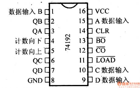
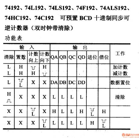
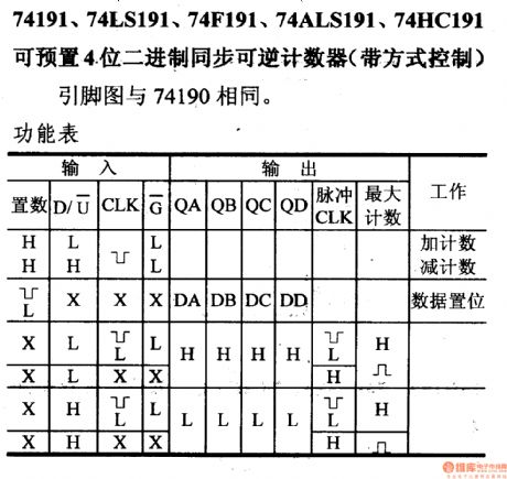
74 Series digital circuit of 74192,74L192 preset BCD decimal synchronous reversible counter(dual clock with clear)
Published:2011/8/1 0:45:00 Author:Lucas | Keyword: 74 Series , digital circuit , preset BCD decimal , synchronous reversible counterd, ual clock with clear
View full Circuit Diagram | Comments | Reading(3465)
CMOS_PROGRAMMABLE_DIVIDE_BY_N_COUNTER
Published:2009/6/28 21:53:00 Author:May
Circuit Notes
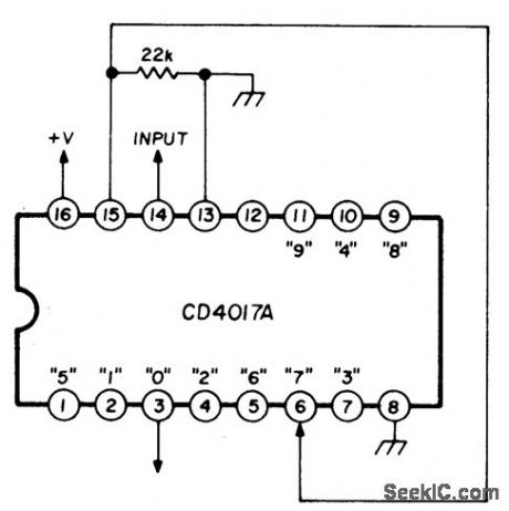
A single connection change permits division by any integer between 2 and 10. The RCA CD4017A Johnson decade counter is shown connected as a divide by 7 counter. The resistor is used to hold the reset line low. When the appropriate number is reached, that output and the reset line are driven high, resetting the counter. To divide by other integers, pin 15 should be connected to the desired output. For example, pin 1 for a divide by 5, or pin 7 for a divide by 3. The output of the divider appears on the 0 line. (View)
View full Circuit Diagram | Comments | Reading(1632)
74 Series digital circuit of 74190,74LS190 preset decimal reversible BCD counter(with mode control)
Published:2011/7/31 22:39:00 Author:Lucas | Keyword: 74 Series, digital circuit , preset decimal reversible , BCD counter, mode control

View full Circuit Diagram | Comments | Reading(3731)
CD_IGNITION
Published:2009/6/28 21:50:00 Author:May
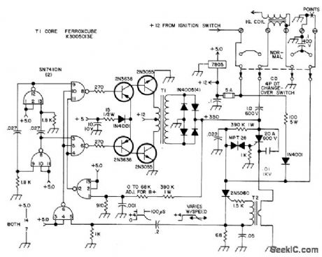
Uses master oscillator-power amplifier type of DC/DC converter in which two sections of triple 3-input NANDgate serve as 10 kHz square-wave MVBR feeding class B PNP/ NPN power amplifier through two-gate driver. Remaining two gates are used as logic invert-ers. Secondary of T1 has t5.24 meters of No. 26 in six bankwindings, with 20tums No. 14 added and center-tapped for primary. T2 is unshielded iron-core RF choke, 30-100 pH, whh several turns wound over it for secondary. When main 20-A SCR fires, T2 develops oscillation burst for firing sensitive gate-Iatching SCR. Storage ca-pacitor energy is then dumped into ignition coil primary through power SCR.-K. W. Robbins, CD Ignition System, 73 Magazine, May 1974, p 17and19. (View)
View full Circuit Diagram | Comments | Reading(1574)
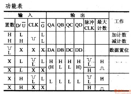
74 Series digital circuit of 74191, 74LS191 preset 4-bit synchronous reversible binary counter(with mode control)
Published:2011/7/31 23:05:00 Author:Lucas | Keyword: 74 Series, digital circuit , preset 4-bit synchronous , reversible binary counter, mode control
View full Circuit Diagram | Comments | Reading(2165)
74 Series digital circuit of 74LS168A/169A preset 4-bit synchronous reversible counter
Published:2011/7/28 22:42:00 Author:Lucas | Keyword: 74 Series , digital circuit , preset 4-bit synchronous , reversible counter
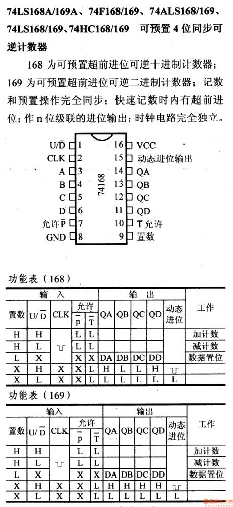
168 is preset carry lookahead reversible decimal counter; 169 is preset carry lookahead reversible binary counter; count and preset are fully synchronized; it can be carry lookahead when fast counting; it can be used for n-bit binary cascade output; the clock circuit is fully independent.
(View)
View full Circuit Diagram | Comments | Reading(1203)
74 Series digital circuit of 74167 BCD synchronization coefficient multiplier
Published:2011/7/29 1:14:00 Author:Lucas | Keyword: 74 Series, digital circuit, BCD , synchronization coefficient multiplier
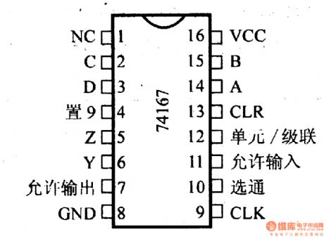
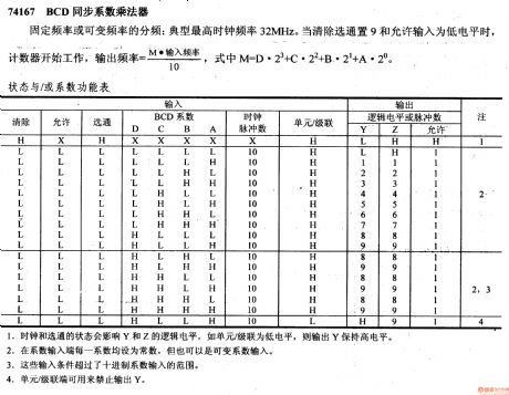
The fractional frequency has the fixed frequency or variable frequency; the typical maximum clock frequency is 32MHz. When the clear strobe sets to 9 and it allows the input to be low, the counter starts to work. 1. The status of clock and strobe has the effect on the logic level Y and Z, for example, unit/ cascade is low, the output Y remains high. 2. Each factor of the factor inputs is set to constant, but also can be a variable factor input. 3. The input conditions have been greater than the decimal input range. 4. Unit/cascade can be used to disable the output terminal Y.
(View)
View full Circuit Diagram | Comments | Reading(1347)
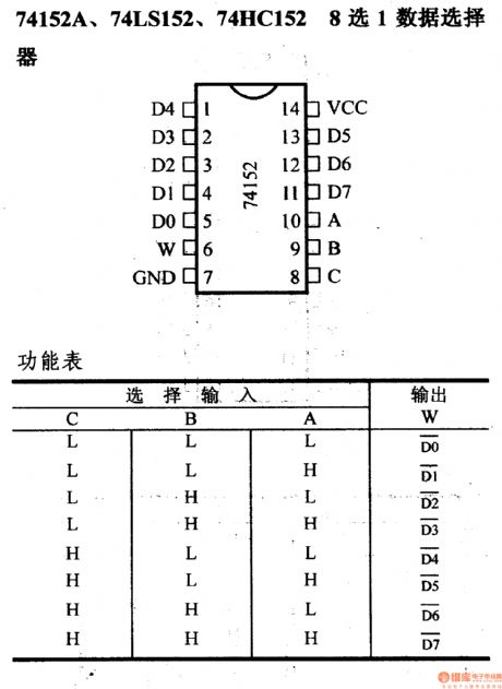
74 Series digital circuit of 74152A, 74LS152 8-to-1 data selector
Published:2011/7/25 3:51:00 Author:Lucas | Keyword: 74 Series , digital circuit, 8-to-1 data selector
View full Circuit Diagram | Comments | Reading(1199)
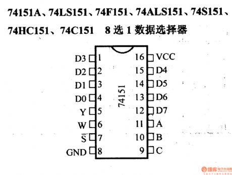
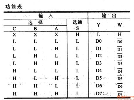
74 Series digital circuit of 74151A, 74LS151 8-to-1 data selector
Published:2011/7/25 3:52:00 Author:Lucas | Keyword: 74 Series, digital circuit , 8-to-1 data selector
View full Circuit Diagram | Comments | Reading(4288)
74 Series digital circuit of 74148,74LS148 8-3 line priority encoder
Published:2011/7/25 3:54:00 Author:Lucas | Keyword: 74 Series , digital circuit , 8-3 , line priority encoder
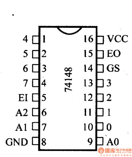
View full Circuit Diagram | Comments | Reading(10090)
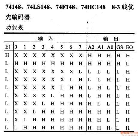
74 Series digital circuit of 74147,74LS147 decimal 4 line BCD priority encoder
Published:2011/7/25 3:57:00 Author:Lucas | Keyword: 74 Series , digital circuit , decimal 4 line , BCD priority encoder
View full Circuit Diagram | Comments | Reading(4739)
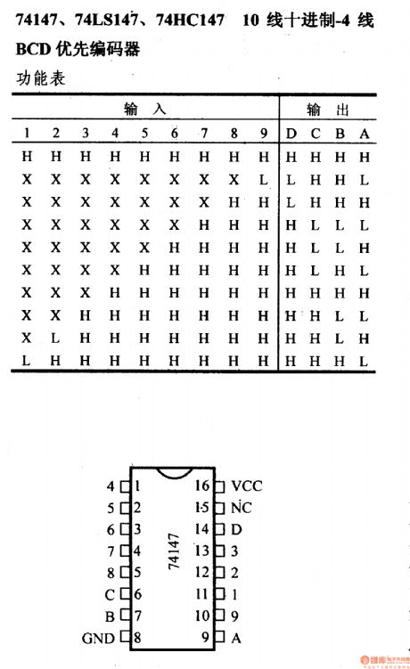
74 Series digital circuit of 74145,74LS145 BCD decimal decoder / driver (OC)
Published:2011/7/25 4:01:00 Author:Lucas | Keyword: 74 Series , digital circuit , BCD decimal decoder , BCD decimal driver , OC
It is used to drive lamp, relay or MOS circuit; it can absorb 80mA current; the typical power consumption of LS145 is 35mW; withstand voltage is 15V.
(View)
View full Circuit Diagram | Comments | Reading(2531)
HEADLIGHT_REMINDER
Published:2009/6/28 21:21:00 Author:May
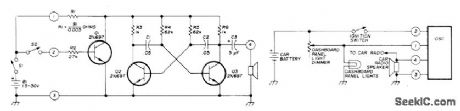
Uses basic oscillator consisting ofQ2 and Q3 arranged as collectorcoupled astable MVBR. Power is taken from collector of Q1 which acts as switch for Q2 and Q3. With S1 closed and S2 open, oscillator operates. Closing S2 saturatesQ1 and stops oscillator. When used as headlight reminder for negativeground car, B1 is omitted and power for oscillator is taken from dashboard panel lights since they come on simultaneously with either parking lights or headlights. If ignition key is turned on, al saturates and disables Q2-Q3. With ig-nition off but lights on, Q1 is cut off and oscillator receives power. Audio output may be connected directly to high side of voice coil of car radio loudspeaker without affecting operation of radio. Almost any NPN transistors can be used. Changing values of R4 and R5 changesfre-quency of reminder tone.-H. F. Batie, Versatile Audio Oscillator, Ham Radio, Jan. 1976, p 72-74. (View)
View full Circuit Diagram | Comments | Reading(851)
SOUND_ACTIVATED_STROBE_TRIP
Published:2009/6/28 20:57:00 Author:May
Take strobe-flash pictures the instant a pin pricks a balloon, a hammer breaks a lamp bulb or a bullet leaves a gun. Use a transistor amplifier of 1-watt rating or less. (It must have an output transformer.) The amplifier is terminated with a resistor on its highest output impedance, preferably 16 ohms. To test, darken room lights, open camera shutter, and break a lamp bulb with a hammer. The sound of the hammer striking the lamp will trigger the flash, and the picture will have been taken at that instant. (View)
View full Circuit Diagram | Comments | Reading(0)
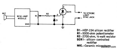
SOUND_LIGHT_FLASH_TRIGGER
Published:2009/6/28 20:55:00 Author:May
Sound input to the microphone triggers tthe IC monostable circuit which subsequently triggers an SCR, and hence the flash, after a time delay. This delay is adjustable—by varying the monostable on-time—from from 5 milliseconds to 200 milliseconds. (View)
View full Circuit Diagram | Comments | Reading(0)
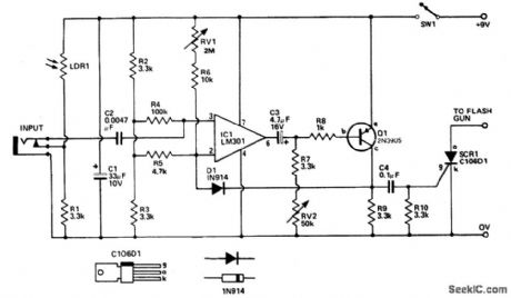
PHOTO_STOP_ACTION
Published:2009/6/28 20:52:00 Author:May
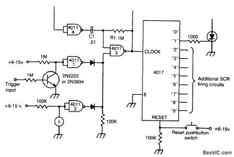
This circuit gives multiple stop-action photographic effects like showing a bouncing ball in up to nine locations in a single photograph. The circuit will automatically fire the bulbs sequentially with the time between each firing variable. The circuit is functionally complete except for the actual firing system. In many cases, a simple SCR will work, as shown. The firing can be initiated in one of two ways. A trigger pulse can be applied to the trigger input terminal through a capacitor, or can operate the unit as a slave. Light from a camera-mounted flash will activate the circuit through its built-in photocell pickup. The time period between each successive flash is determined by C1 and R1, which is variable. Afterfiring the circuit, it must be reset by momentarily depressing the reset button. (View)
View full Circuit Diagram | Comments | Reading(993)
DUAL_VOLTAGE_RECTIFIER_CIRCUIT
Published:2009/6/26 4:27:00 Author:May
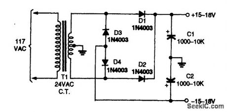
This stepped-up dual voltage supply provides ±15 to ±18V unregulated. (View)
View full Circuit Diagram | Comments | Reading(836)
lO_MHz_COAXIAL_LINE_DRIVER
Published:2009/6/26 4:22:00 Author:May
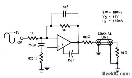
The circuit will find excellent usage in high frequency line driving systems that re-quire wide-power bandwidths at high output current levels. (IC = HA2530) The bandwidth of the circuit is limited only by the single pole response of the feedback components; namely f(-3 dB) = 1/2 πRfCf. As such, the response is flat with no peaking and yields minimum distortion. (View)
View full Circuit Diagram | Comments | Reading(863)
24_V_TO_33_V_SWITCHING_REGULATOR
Published:2009/6/26 4:08:00 Author:May
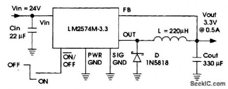
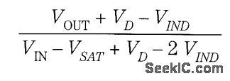
The National Semiconductor LM2574 delivers 3.3 V out at O.SAfrom a 24-V source. The duty cycle is:VD = diode drop(0.39)VIND = inductor dc dropVSAT = saturation voltage of LM2574(0.9 V typical) (View)
View full Circuit Diagram | Comments | Reading(0)
5_V_TO_33_V_SWITCHING_REGULATOR
Published:2009/6/26 4:05:00 Author:May
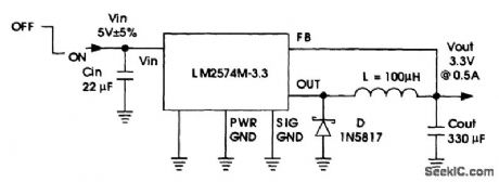
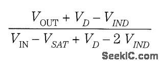
A National Semiconductor LM2574 is used to derive 3.3 V at 0.5 A from a 5-V logic bus. The duty cycle is: VD = diode drop (0.39) VIND = inductor dc drop VSAT = saturation voltage of LM2574 (0.9 V typical) This circuit should be useful to derive 3.3 V for logic devices from existing +5-V buses. (View)
View full Circuit Diagram | Comments | Reading(0)
| Pages:6/19 12345678910111213141516171819 |
Circuit Categories
power supply circuit
Amplifier Circuit
Basic Circuit
LED and Light Circuit
Sensor Circuit
Signal Processing
Electrical Equipment Circuit
Control Circuit
Remote Control Circuit
A/D-D/A Converter Circuit
Audio Circuit
Measuring and Test Circuit
Communication Circuit
Computer-Related Circuit
555 Circuit
Automotive Circuit
Repairing Circuit