
Digital Circuit
Index 15
MINUTE_MARKER
Published:2009/6/19 1:54:00 Author:May
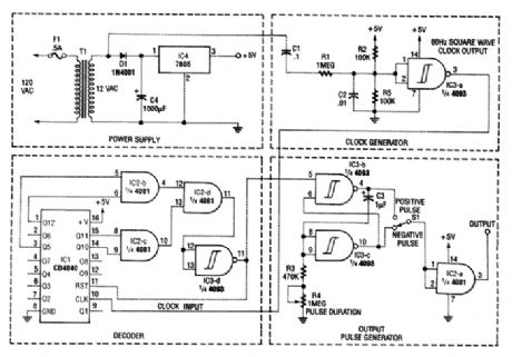
The figure shows the schematic of a minute marker. The output of transformer T1 is 12.6 Vac at 60 Hz, which is rectified by D1 and regulated by IC4, and LM7805 regulator, to provide 5 Vdc for the circuit. The unrectified ac is bandpass-filtered by R1, R2, R5, C1, and C2. Resistors R2 and R5 also form a dcvoltqge divider, which biases the input of Schmitt trigger IC3-a to 2.5 V. The Schrnitt trigger generates a 60-Hz square wave, which is fed to the input of IC1, a CE4040 12stage binary counter.The outputs of the counter are a 4081 quad AND gate (IC2), and the decoded output is fed back to the reset input of the counter, which resets the counter when the desired count is reached.The pulse from IC2-d is inverted by Schmitt trigger IC3-d, and passed along to the output pulse generator. The output pulse is generated by two Schmitt triggers cross-connected as an RS flip-flop (IC3-b and IC3-c). The output of the flip-flop is fed to 3, R4, and C3, whose values set the output pulse duration. The output pulse duration (T) can be approximated by the formula T=1.2×C3×(R3+ R4).A positive or negative-going pulse is selected by 51, and buffered by the remaining AND gate (IC2-a). (View)
View full Circuit Diagram | Comments | Reading(902)
FREQUENCY_BASED_LOCK
Published:2009/6/19 1:38:00 Author:May
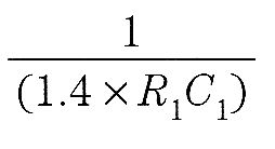


The system is formed by two separate circuits-a key and a keyhole. The key engages the key-hole with a mating pair of connectors. The key is a tone-generator circuit consisting of a 4049 hex in-verter CMOS IC (U1), switches (S1 and S2), a resistor (R1), and a capacitor (C1). The value of the tone generated by that circuit in Hz is determined by;The keyhole is a 567 tone-decoder circuit that can be conftgured to detect any frequency from 0.01 Hz to 500 kHz. The frequency it detects (fo), via the 567 IC, turns on the relay (K1). Compo-nents R3 and D1 are used to latch the circuit, so the output stays on even after the input tone is re-moved. When S2 is pressed, the system is reset. Switch S3 resets the circuit from inside. (View)
View full Circuit Diagram | Comments | Reading(987)
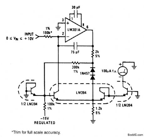
LOW_COST_ACCURATE_SQUARING_CIRCUIT
Published:2009/6/18 5:12:00 Author:May
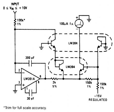
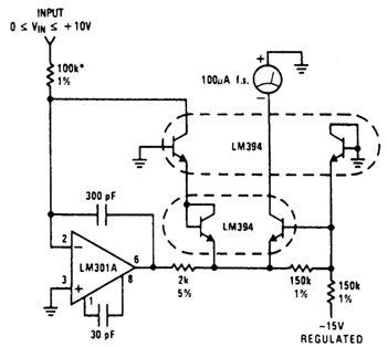
The circuit shown will square the input signal and deliver the result as an output current.Full-scale input is 10V,but this can be changed simply by changing the value of the 100-kQ input resis-tor.As in the square root Gircuit, the -15-V supply is used as the reference. In this case, however, a 1% shift in supply voltage produces a 1% shift in the output signal.The 150-kQ resistor across the base-emitter of 1/2LM394 provides slight temperature compensation of the reference current from the -15-V supply.For improved accuracy at low input signal levels,the offset voltage of the LM301A should be zeroed out,and a 100-kQ resistor should be inserted in the positive input to provide input to provide optimum dc balance. (View)
View full Circuit Diagram | Comments | Reading(840)
VERY_EFFICIENT_SOLENOID_DRIVER
Published:2009/6/18 4:59:00 Author:May

In the circuit shown, the IC in the center, U1, contains a microprocessor-compatib le serial-in, parallel-out shift register, with strobed latch and high-level solenoid drives (see the figure).The strobe pulse turns on the selected loads at full power for its pulse width, which is 0.5 sec-ond. Following the strobe pulse, the driver outputs are pulse-width modulated by the multivibrator, which is set for a duty cycle of 25%. The solenoids are therefore held in the engaged position with a voltage that's 25% of the nominal supply voltage.U2B acts as the basic multivibrator in the circuit, and U2A sets the duty cycle by setting the dis-charge current of capacitor C1. U2D overrides the oscillation during the strobe pulse. And U2C pro-vides the Power-On Reset (POR), inhibiting the solenoid loads from turning on during the initialization period of the microprocessor. (View)
View full Circuit Diagram | Comments | Reading(1378)
27125_MHz_NBFM_TRANSMITTER
Published:2009/6/18 4:44:00 Author:May
Using a Motorola MC2833 one-chip FM transmitter, a few support components, and an MPF6660 FET RF amp, this trans-mitter delivers about 3 W into a 50-Ω load. It is capable of operation over about 29 to 32 MHz with the components shown. (View)
View full Circuit Diagram | Comments | Reading(1535)
IMPEDANCE_MATCHED_LINE_DRIVER_WIHH_75_Ω_LOAD
Published:2009/6/18 4:31:00 Author:May
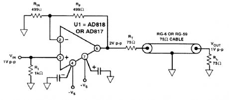
This circuit is a wideband 75-Ω line driver, for video applications (1 V p-p into 75Ω). (View)
View full Circuit Diagram | Comments | Reading(620)
LOW_COST_ACCURATE_SQUARE_ROOT_CIRCUIT
Published:2009/6/18 4:21:00 Author:May
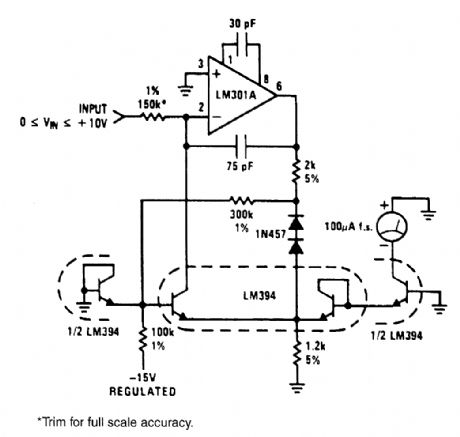

The circuit will generate a square-root function, accurately and inexpensiveJy. The output is a current that can be used to drive a meter directly or be converted to a voltage with a summing junc-tion current-to-voltage converter. The-15-V supply is used as a reference, so it must be stable. A 1% change in The-15-V supply will give a 1/2% shift in output reading. No positive supply is required when an LM301A is used because its inputs can be used at the same voltage as the positive supply (ground). The two 1N457 diodes and the 300-kΩ resistor are used to temperature-compensate the current through the diode-connected1/2 LM394. (View)
View full Circuit Diagram | Comments | Reading(1586)
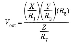
LOW_COST_ONE_QUADRANT_MULTIPIER_DIVIDER
Published:2009/6/18 4:02:00 Author:May


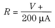
This circuit will produce an output that is proportional to the product of the (JQ and ()] inputs divided by the Z input. All inputs must be positive, limiting operation to one quadrant.For very low level inputs, the offset voltage in the LM308s might create large percentage errors referred to input. A simple scheme for offsetting any of the LM308s to zero is shown in dotted line; the positive input of the appropriate LM308 is simply tied toRX instead of ground for zeroing. The summing mode of operation on all inputs allows easy scaling on any or all inputs. Simply set the input resistor equal to (Vin(max)/200μA). Vout is equal to:Input voltages above the supply voltage are allowed because of the sumrning mode of operation. Several inputs can be summed at X,Y,and Z.For a simple {X)·(Y) or (X)/Z function, the unused input must be tied to the reference voltage. Perturbations in this reference will be seen at the output as scale factor changes, so a stable refer-ence is necessary for precision work. For less critical applications, the unused input can be tied to the positive supply, with (View)
View full Circuit Diagram | Comments | Reading(878)
TWO_TONE_ENCODER
Published:2009/6/18 3:49:00 Author:May
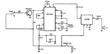
Using an XR2206 oscillator, this circuit can generate two audio tones. Switching between tones can be done with a logic level to either the base of the PN2222 or pin 9 of the XR2206. (View)
View full Circuit Diagram | Comments | Reading(0)
RELAY“OR”CIRCUIT
Published:2009/6/18 3:41:00 Author:May
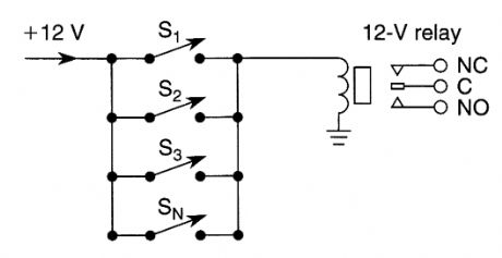
Closing any switch S1,S2,S3,or Sn will actuate the relay(N=any number).Use this circuit for burglar alarms,etc. (View)
View full Circuit Diagram | Comments | Reading(626)
RELAY“AND”CIRCUIT
Published:2009/6/18 3:37:00 Author:May
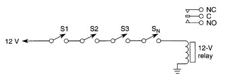
All switches 51 through Sn must be closed to operate the relay.If one opens,the relay drops out.Use this circuit for burglar alarms,etc. (View)
View full Circuit Diagram | Comments | Reading(633)
SIMPLE_IDENTIFIER
Published:2009/6/18 3:30:00 Author:May
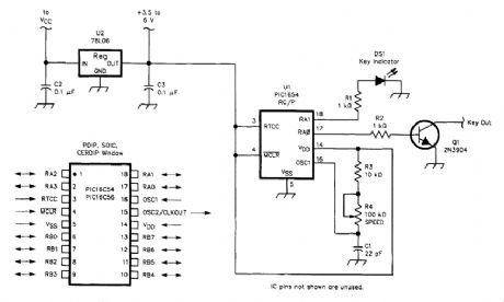
This identifier uses a PIC 16C54 microcontroller which must be programmed for your desired identifier. (View)
View full Circuit Diagram | Comments | Reading(1426)
AND_GATE
Published:2009/6/18 3:29:00 Author:May
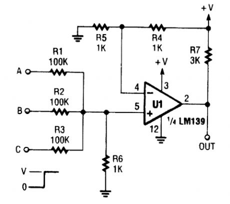
An LM1139 is configured as an AND gate(TTL or CMOS is usually used).use leftover IC sections and save an extra package in some instances. (View)
View full Circuit Diagram | Comments | Reading(0)
PF_LINE_SAMPLER_COUPLER
Published:2009/6/18 3:02:00 Author:May
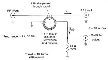
Suitable for RE line sampling, this coupler is useful where an indirect measurement of line cur-rent is needed. A 10:1 turn ratio yields a secondary current about1/10 (ideally) of the line current. A 51-Ω, resistor terminates the secondary. Insertion loss in the main line is negligible, < 0.l dB. For higher power levels, use proportionately larger core for T1. (View)
View full Circuit Diagram | Comments | Reading(731)
VOLTAGE_LEVEL_CIRCUIT
Published:2009/6/17 21:47:00 Author:May
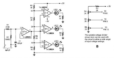
A DC op amp and a comparator with a ladder reference divider allow a dc input voltage to light one or more LEDs, depending on voltage levels. (View)
View full Circuit Diagram | Comments | Reading(1113)
LOAD_SENSING_TRIGGER
Published:2009/6/17 3:18:00 Author:May

A device plugged into S01 causes a voltage-limited gate trigger for triac TR1, and causes power to be applied to SC2. (View)
View full Circuit Diagram | Comments | Reading(993)
TRANSISTORIZED_SCHMITT_TRIGGER
Published:2009/6/17 2:49:00 Author:May

View full Circuit Diagram | Comments | Reading(1181)
CODE_PRACTICE_OSCILLATOR_USES_OPTOISOLATOR
Published:2009/6/17 2:37:00 Author:May
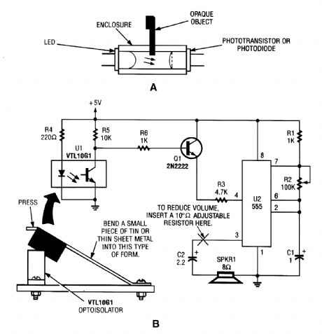
A slotted-pair isolator (A) is effectively an enclosed-pair isolator with a slit that will allow an obstacle to interrupt the light path. That could be useful for building a code key (B). (View)
View full Circuit Diagram | Comments | Reading(991)
CARRIER_CURRENT_BABY_ALERT_RECEIVER
Published:2009/6/17 2:25:00 Author:May
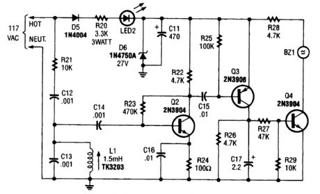
The baby-alert receiver is comprised of three transistors: Q2, which is configured as a high-gain linear amplifier; Q3, which serves as both an amplifier and detector; and Q4, which is essentially used as a switch; and a few additional components. It sounds an alarm BZ1 on receipt of a 125-kHz signal from an alarm transmitter via the 120-V power lines. (View)
View full Circuit Diagram | Comments | Reading(737)
VISIBLE_LIGHT_RECEIVER
Published:2009/6/17 1:41:00 Author:May
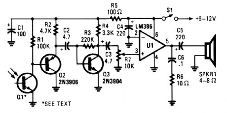
This receiver for amplitude-modulated light signals uses phototransistor Q1 mounted in a para-bolic reflector (to increase range). Any npn phototransistor should work. Emitter-follower Q2 drives amplifier Q3. The output from Q3 feeds volume control R7 and audio amplifier UI. A 9- to 12-V supply is recommended for the receiver. (View)
View full Circuit Diagram | Comments | Reading(1067)
| Pages:15/19 12345678910111213141516171819 |
Circuit Categories
power supply circuit
Amplifier Circuit
Basic Circuit
LED and Light Circuit
Sensor Circuit
Signal Processing
Electrical Equipment Circuit
Control Circuit
Remote Control Circuit
A/D-D/A Converter Circuit
Audio Circuit
Measuring and Test Circuit
Communication Circuit
Computer-Related Circuit
555 Circuit
Automotive Circuit
Repairing Circuit