
Index 188
BATTERY_SAVING_TIMER
Published:2009/7/13 1:32:00 Author:May
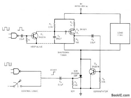
Developed for use with alarms, remote controls, or unattended electronic equipment, to turn off battery auto-matically at predetermined interval after circuit is actuated by control logic or switch. Turn-on applies positive pulse that triggers SCR on, grounding load and UJT timer Q2. After delay interval determined by values of C1 and R1, Q2 fires and discharges C1, producing pulse across R, that tums on Q3. This in tum shunts SCR and commutates it off. Circuit is thus turned off, after which only very small leakage currents through reverse SCR junction will be drain on battery.-D. Weigand, Battery Saver Has Automatic Tum-Off, EDN Magazine, April20, 1973, p91. (View)
View full Circuit Diagram | Comments | Reading(694)
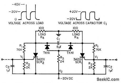
DUAL_FUNCTION_BISTABLE_SCRAM
Published:2009/7/13 1:19:00 Author:May
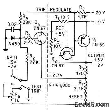
Porlion at right of dotted lines acts as regulator that holds constant voltage on output circuit until tripping of control rods is called for by nuclear radiation detector.Outputs of bistable circuits are connected through and gates so that, if desired, two input signals are necessary before trip signcd is generated. Malfunction in ion chambers or failure of circuit component can make reactor exceed maximum critical assembly condition and generate trip signal that drops control rods.-E. J.Wade and D.S. Davidson, How Transistor Circuits Protect Atomic Reactors, EJectronics, 31:29,73-75. (View)
View full Circuit Diagram | Comments | Reading(975)
TWO_TERMINAL_PIEZO_DEVICE_DRIVER
Published:2009/7/13 0:09:00 Author:May
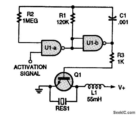
Two-terminal devices can be driven by two NAND gates. A booster coil is used to compensate for the sound-pressureattenuation caused by the case. (View)
View full Circuit Diagram | Comments | Reading(805)
LOW-DISTORTION_LINE_DRIVER
Published:2009/7/13 0:06:00 Author:May
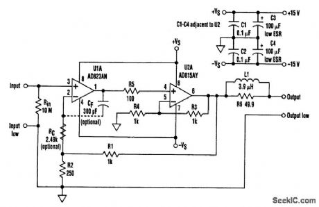
This low-distortion driver circuit delivers up to ±0.5 A and is suitable for loads of 10Ω and up. Using a low-offset, low-bias-current input stage, the driver can be entirely direct-coupled. Gain is equal to 1+R2/R1. (View)
View full Circuit Diagram | Comments | Reading(813)
TRANSIENT_ELIMINATOR
Published:2009/7/13 0:06:00 Author:May
Used between DC power supply and load to eliminate supply transients that might damage semiconductor devices. Zener rating should be about 10% higher than supply voltage so Q1 is normally turned off. Q2 is normally conducting. When voltage spike is present on input line, zener conducts and turns Q1 on. Q1 then places positive bias on 10K pot to turn off Q2 and protect load during transient.-J. Fisk, Circuits and Techniques, Ham Radio, June 1976, p 48-52. (View)
View full Circuit Diagram | Comments | Reading(966)
SPARK_MACHINING_SERVO_DRIVE
Published:2009/7/13 0:03:00 Author:May
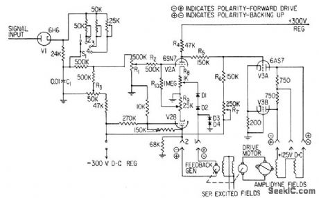
Posilioning information is derived from gap voltage, fed to integrating circuit through diode V1, and resuhing output fed through V2 to cath-ode-coupled push-pull d-c amplifier that excites field of amplidyne generator to move tool electrode toward or away from work-piece, as required to permit sparkover at voltage selected for machining conditions desired. Used chiefiy for work on high-tempemture alloys and otherwise unmachinoble materials.-E. M. Williams and C. P. Porterleld, Spark Machine Tool has Servo Control, Electronics,31:43,p90-92. (View)
View full Circuit Diagram | Comments | Reading(1182)
TEAl504 switching power control circuit diagram
Published:2011/8/4 2:14:00 Author:Ecco | Keyword: switching power control
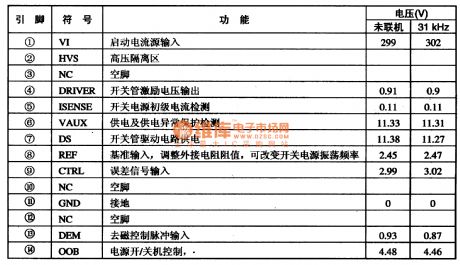
TEAl504 new switching power supply control IC produced by Philips, which is the core component to form the separately excited switching power supply, and they are widely used in color television sets, computers and color monitors, and other electrical power supply circuits. TEA1504 integrated circuit includes start-up circuit, switch drive circuit, power supply circuit, oscillation frequency control circuit, power on / off control circuit, switch circuit incentives, and other auxiliary circuits.
(View)
View full Circuit Diagram | Comments | Reading(578)
CONSTANT_CURRENT_SOURCE_CONVERTER
Published:2009/7/13 0:03:00 Author:May
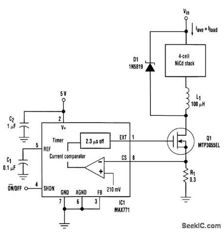
To maintain regulation, the switching voltage regulator shown includes independent loops of current and voltage feedback. If the voltage loop is disabled, the current loop can be used to implement a general-purpose current source. The first step in obtaining a current source is to apply 5 V to V+. Because the chip expects 12 V of feedback at that terminal, it assumes a loss of regulation and shifts control to the current loop. This mode of operation allows an increasing ramp of current through Q1, causing the voltage at pin 8 to increase until it reaches the internal comparator threshold (210 mV). Timing circuitry then turns off Q1 for a fixed 2.3 μs, and the cycle repeats. The result is a relatively constant inductor current, which also happens to be the load current.With a proper choice of component values, the circuit generates constant current over a wide range of input voltages. The circuit (with component values shown) is a fast charger for NiCd batteries that provides 60-mA charging currents. (View)
View full Circuit Diagram | Comments | Reading(2120)
1200_1_PULSE_WIDTH_MONO
Published:2009/7/16 13:07:00 Author:Jessie
Output pulse width at collector of Q2 can be varied from 0.5 to 300 millisec. With suitable trigger, serves as one-shot for variety of uses.-Wide Range Variable Multivibrator, Electronic Circuit Design Handbook, Mactier Pub. Corp., N.Y., 1965, p 110. (View)
View full Circuit Diagram | Comments | Reading(706)
IMPROVED_TRIGGERING_OF_MONO
Published:2009/7/16 13:06:00 Author:Jessie
Addition of three diodes and one resistor to conventional monstable mvbr permits increasing value of timing resistor Rt without making circuit susceptible to false triggering.-H. Cohen, Eliminating False Triggering in Monostable Multis, EEE, 14:8, p 168. (View)
View full Circuit Diagram | Comments | Reading(641)
FAST_TURNOFF_MONO
Published:2009/7/16 13:05:00 Author:Jessie
Has long delay time along with fast rise and fall times (each 30 nsec). Pulse amplitude is clamped at 5 V.-Fast Turnoff Monostable Multivibrator, Electronic Circuit Design Handbook, Mactier Pub. Corp., N.Y., 1965, p 69. (View)
View full Circuit Diagram | Comments | Reading(751)
HIGH_POWER_ASTABLE
Published:2009/7/16 13:03:00 Author:Jessie
Simple astable circuit design eliminates external trigger, minimizing number of components. Voltage dividers R1 and R2 provide gate voltage for scr's. Both dividers start charging associated capacitors C2 until one scr breaks down, initiating oscillation. Used in converter power supplies.-W. B. McCartney and E. O. Uhrig, Actable High Power Multivibrator, EEE, 10:12, p 30-31. (View)
View full Circuit Diagram | Comments | Reading(1030)
SINGLE_SHOT_FOR_SHMOO_PLOTTER
Published:2009/7/16 12:41:00 Author:Jessie
Used for automatic testing of computer memories under marginal drive currents, Error in memory causes monostable mvbr to generate pulse half as long as complele pass through storage, to make system track along error boundry. Npn transistors are 2N706 and the diode is 1N921.-J. E. Gersbach, The Great Shmoo Plot: Testing Memories Automatically, Electronics, 39:15, p 127-134. (View)
View full Circuit Diagram | Comments | Reading(728)
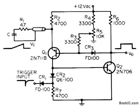
POWER_ONE_SHOT
Published:2009/7/16 12:40:00 Author:Jessie

Complementary-symmetry one-shot supplies 1.4 W for 0.1 sec to relay coil on very low duty cycle, without drawing standby power. Used to discharge large 10-kv capacitor. -W. P. Mitchell, Power One-Shot, EEE, 13:6, p 68. (View)
View full Circuit Diagram | Comments | Reading(736)
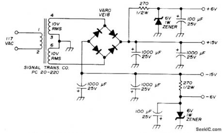
±6_V_AND_±15_V
Published:2009/7/13 Author:May
Suitable for use when frequency or some other critical parameter of load is not dependent on voltage. Developed for use in CMOS IC function generator.-R. Megirian, Ingegrated-Circuit Function Generator, Ham Radio, June 1974, p 22-29. (View)
View full Circuit Diagram | Comments | Reading(1137)
DOUBLE_COUPLED_MAIN_GATE_MVBR
Published:2009/7/16 12:37:00 Author:Jessie
Uses both cathode and plate-to-grid coupling, with gate length changed by switching of potentiometers. Used in radar to provide gate during which display sweep is generated, along with gates for waveforms that must be coincident with display sweep.-NBS, Handbook Preferred Circuits Navy Aeronautical Electronic Equipment, Vol. 1, Electron Tube Circuits, 1963, p N10-3. (View)
View full Circuit Diagram | Comments | Reading(576)
230_VAC_FROM_115_VAC
Published:2009/7/12 23:55:00 Author:May
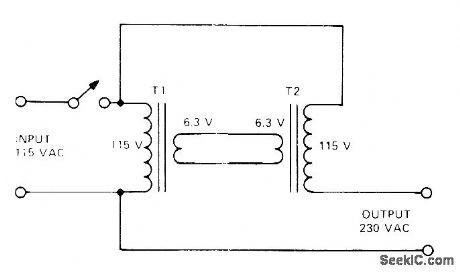
Connect 6.3-V filament transformers back.to-back as shown to get 230 V when step-up transformer is not available. 115-V windings must be phased properly in series; if wrong, output voltage will be zero.Output power rating at 230 V is somewhat less than twice the power (E x I) rating of smallest filament transformer. If 6.3-V 10-A transformers are used, power rating would be about 1000 W (less than 2 x 6.3 x 10).-A. E. McGee, Jr., Cheap and Easy 230 Volt AC Power Supply, 73 Magazine, Aug. 1974, p 64. (View)
View full Circuit Diagram | Comments | Reading(1251)
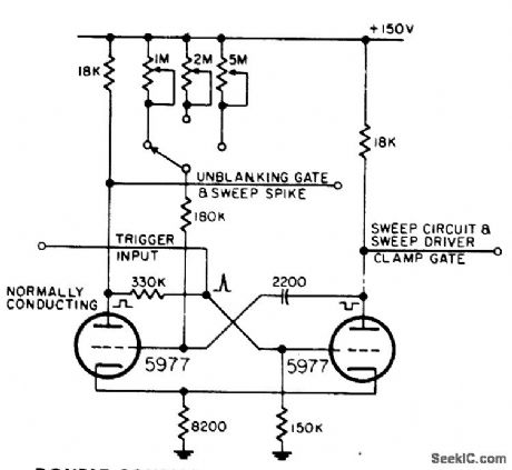
CATHODE_COUPLED_MAIN_GATE_MVBR
Published:2009/7/16 12:37:00 Author:Jessie
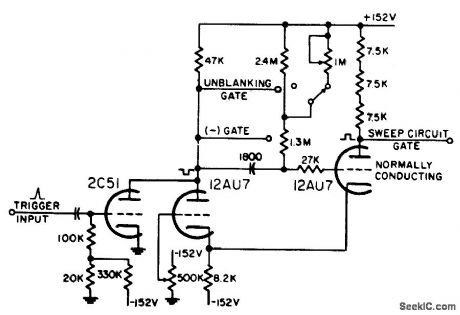
Positive gate is d-c coupled from plate of normally-on tube to cathode follower whose cathode resistor is common with diode clamp of main-gate mvbr. Negative gate for unblanking is taken from plate that is a-c coupled to opposite grid of mvbr.-NBS, Handbook Preferred Circuits Navy Aeronautical Electronic Equipment, Vol. 1, Electron Tube Circuils, 1963, p N10-2. (View)
View full Circuit Diagram | Comments | Reading(566)
FAST_RECOVERY_ONE_SHOT_1
Published:2009/7/16 12:02:00 Author:Jessie
Pulse width can be varied from 0.1 microsec to 10 millisec in decade ranges by changing timing capacitors. Used in commercial radar range unit and in pulse analyzer.-J. Rogers, Fast-Recovery One-Shot Multi Gives 10:1 Width Control, EEE, 14:4, p 44-45. (View)
View full Circuit Diagram | Comments | Reading(552)
THUMBWHEEL_SET_TO_99_min
Published:2009/7/12 23:52:00 Author:May
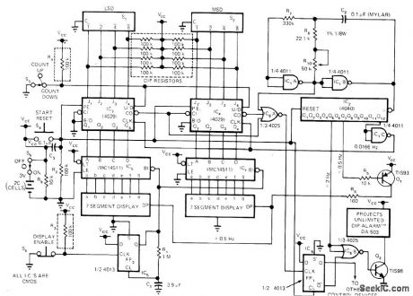
Developed for timing events and for limiting event to predetermined interval that can be set up with 2-digit BCD-encoded thumbwheel switches. Digital display shows time remaining, as guide for speakers. Audible alarm indicates end of time interval. Flashing decimal point indicates counter is working. Designed for operation from two C cells. To conserve power, display is normally blanked; pressing display-enable switch turns on display for about 4 s Article describes operation of circuitin detail,-R.A.Fairman, CMOS Lowers Timer Power Consurnption,EDN Magazine,Oct.5,1975,p78 and 80. (View)
View full Circuit Diagram | Comments | Reading(850)
| Pages:188/471 At 20181182183184185186187188189190191192193194195196197198199200Under 20 |
Circuit Categories
power supply circuit
Amplifier Circuit
Basic Circuit
LED and Light Circuit
Sensor Circuit
Signal Processing
Electrical Equipment Circuit
Control Circuit
Remote Control Circuit
A/D-D/A Converter Circuit
Audio Circuit
Measuring and Test Circuit
Communication Circuit
Computer-Related Circuit
555 Circuit
Automotive Circuit
Repairing Circuit