
Index 194
THIN_FlLM_CURRENT_DRIVER
Published:2009/7/12 21:20:00 Author:May
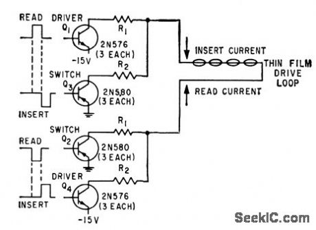
Three 2N576 driver transistors in parallel, each rated 400 ma, deliver 1-amp pulses with 0.15 microsec rise time. Three 2N580 pnp transistors in pamllel serve as current switches.-E. E. Bittmann, Using Thin Films in High-Speed Memories, Electronics,32:23,p55-57. (View)
View full Circuit Diagram | Comments | Reading(509)
WIRELESS_FM_MICROPHONE
Published:2009/7/12 21:17:00 Author:May
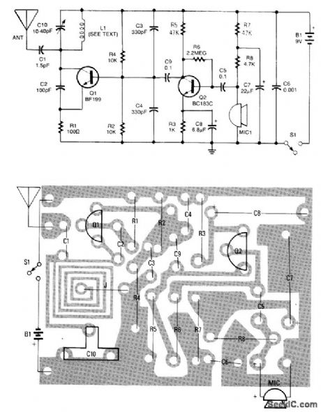
A simple FM wireless microphone uses a single BC183C transistor as an audio amplifier. A 2N3565 can be substituted. Q1 is an oscillator that is FM modulated by the signal from Q1. Other transistors can be substituted, but the modulation characteristics should be checked. (View)
View full Circuit Diagram | Comments | Reading(0)
THIN_FILM_MEMORY_DRlVER
Published:2009/7/12 21:16:00 Author:May
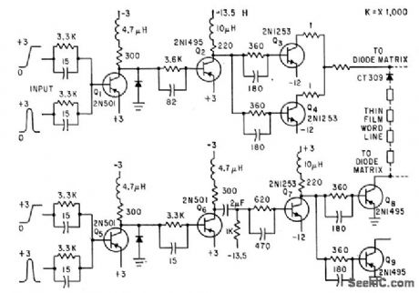
Generales l-amp pulses with 35-nsec rise and fall times, at rates up to 1 Mc, for driving 2,560-bit memory plane using 2,000-angstrom nickeliron films.-E. E. Bittmann, Ihin Magnetic Film Memories for High-Speed Computers, Electronics, 34:9, p39-41. (View)
View full Circuit Diagram | Comments | Reading(564)
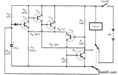
TRANSISTOR_RADIO_TURNOFF
Published:2009/7/12 21:15:00 Author:May

Circuit switches radio off after delay of about 30 min, if ganged switch is set to other position and radio switch itself is left on. Current drain of timer circuit is negligible in both positions. Article describes timing action of transistors in detail. Tr1 should have current gain above 25 with collectorcurrents of 10 to 100 mA; 2N3706 can be used here and for Tr5. Other transistors should have current gain above 50, as in 2N3702. For operation from 4.5 to 9 V, omit diode and cut values of R4-R7 in half.-S. Lamb, Delayed Switch Off for Transistor Radios, Wireless World, Aug. 1973, p 373. (View)
View full Circuit Diagram | Comments | Reading(917)
15_min_DELAY
Published:2009/7/12 21:13:00 Author:May
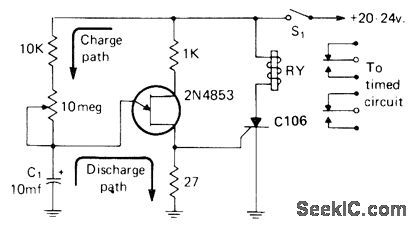
When S1 is closed, C1 begins charging, After delay determined by setting of 10-megohm pot, UJT conducts and makes C1 discharge through 27-ohm resistor, triggering SCR C106 and energizing relay. 0pen S1 to reset circuit.-I, Math, Math's Notes, C0, April 1974, p 64-65 and 91-92.
(View)
View full Circuit Diagram | Comments | Reading(797)
S_R_FLIP_FLOP
Published:2009/7/12 21:13:00 Author:May
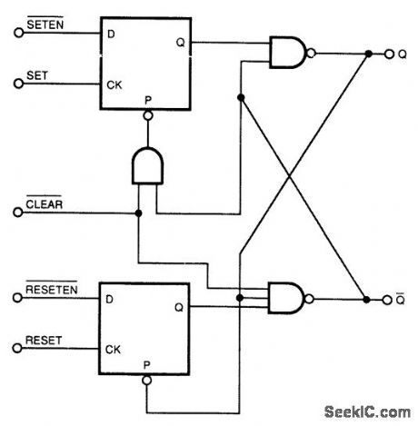
This circuit combines the characteristics of an asynchronous S/R flip-flop and an edge-triggered JK flip-flop. It changes state on the leading edges of its inputs, and ignores the levels at all other times.In operation, outputs of both D flip-flops are normally high, going low for brief periods after seeing an edge at their respective clock inputs. (View)
View full Circuit Diagram | Comments | Reading(985)
SCANNING_KEYBOARD_WITH_MEMORY
Published:2009/7/12 21:12:00 Author:May
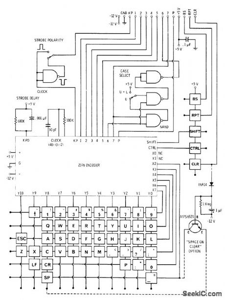
Standard keyboard is updated to 53 keys as required for character feed in microprocessorbased TV typewriter system. Features include two-key rollover, along with choices of letter case, strobe polarity, clear key, and repeat key.Space output is produced automatically during clear.-D. Lancaster, TV Typewriter Cookbook, Howard W. Sams, Indianapolis, IN, 1976.p 150-151. (View)
View full Circuit Diagram | Comments | Reading(659)
FULL_WAVE_RECTIFIER_TO_10_MHz
Published:2009/7/12 21:09:00 Author:May
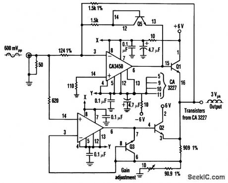
Using two CA3450 op amps and a CA3227 transistor array, this circuit will accurately full-wave rectify signals to 10 MHz. Two of the CA3227 transistors drive the output, two are in the feedback circuits. Two transistors serve as clamping diodes, limit the negative-going signals of each amplifier, and keep both amplifiers active during the end cycle. The maximum output is determined by the slew rate of 300 V/μs at highest frequencies. This output equals 300 V/ms÷6πV peak. (View)
View full Circuit Diagram | Comments | Reading(672)
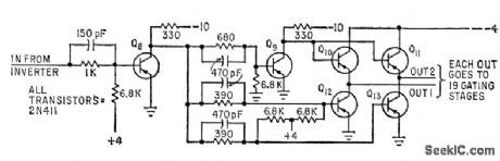
GATE_AND_MIXER_FOR_10_NSEC_PULSES
Published:2009/7/12 21:08:00 Author:May


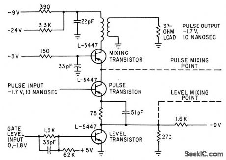
Used in 50-megapulse computer.Propagation delay time of circuit is only 4.5 nsec.Transistors may also be 2N769 or 2N976-K,H.Konkle and J. E. Laynor, Key to Faster Computers:Ten-Nanosecond Amplifer.Electronics,35:50,p39-41. (View)
View full Circuit Diagram | Comments | Reading(491)
HEX_ENCODER_FOR_KEYBOARD
Published:2009/7/12 21:07:00 Author:May
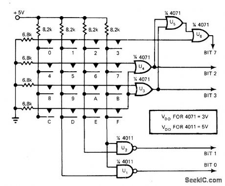
Standard 16-button keyboard is used with CMOS packages to provide hex output bits. Pressing one button increases voltage on its horizontal line from 0 to 2.2 V. If button is in other than first row, OR gate U3 or U4 is activated and either bit 2 or 3 changes from LOW to HIGH. Simultaneously, voltage of vertical column of button decreases from 5 V to 2.2 V. If button is in other than first column, NAND gate U1 or U2 is activated and either bit 0 or 1 changes from LOW to HIGH. OR gates U5 and U6 provide button-pressed signal by changing bit 7 from LOW to HIGH upon activation of any button.-W. H. Hailey, CMOS Logic Implements Keyboard Encoder, EDN Magazine, Aug. 5, 1978, p 54 and 56. (View)
View full Circuit Diagram | Comments | Reading(1626)
10min_ID_TIMER
Published:2009/7/12 21:07:00 Author:May
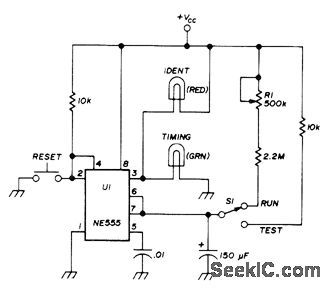
Red pilot lamp comes on at end of timing period, adjustable with R1 from 7 to 11 min, as reminder for amateur radio operatorto makestation identification required by FCC every 10 minutes. Green lamp indicates that timer is on and timing. Lamps should draw no more than 100 mA, to avoid overloading NE555 timer. Any 9-12 VDC supply can be used.-D. Backys, ldentification Timer, Ham Radlio, Nov. 1974, p 60-61. (View)
View full Circuit Diagram | Comments | Reading(694)
FULL_ADDER
Published:2009/7/12 21:06:00 Author:May
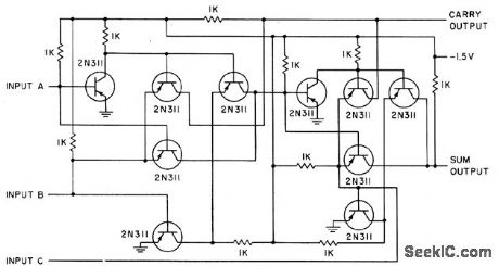
Made by joining two half-adders. Push-pull inverting amplifiers serve as switches to provide completely automatic operation. Carry from full adder can derive from either half-section but never both. No inhibitor signal is required to suppress un wanted sum signal,-F. B. Maynard, Half-Adders Drive Simuhcmeous Computer, Electronics, 31:29, p80-82. (View)
View full Circuit Diagram | Comments | Reading(2041)
RADIO_TURNOFF
Published:2009/7/12 21:05:00 Author:May
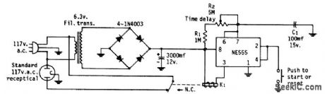
Time-delay control R2 canbe set to turn off radio,TV or other applianceat any desired interval between about 3 and 60 min after start buttonis pushed,ldealfol those who fall asleep to music. K1 is 12-V relay drawing 200 mA ot less.-P. Walton, An Electronic Timer for Less than $5.00, CQ, Aug. 1973, p 42 and 82. (View)
View full Circuit Diagram | Comments | Reading(403)
SIGNAL_CONDITIONER
Published:2009/7/12 21:00:00 Author:May
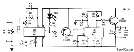
This circuit takes audio from a receiver that might have a weak CW or tone signal and uses a PLL (U1) to recover the weak signal. U1 produces a low on receipt of a tone or note of frequency, determined by R1, R7, and C2. The output of U1 (pin 8) goes low, keys tone generator U2, and produces a new tone. The circuit is useful in cleaning up CW reception in static. noise. etc. (View)
View full Circuit Diagram | Comments | Reading(568)
PRINTER_PORT_D_A_CONVERTER
Published:2009/7/12 20:58:00 Author:May
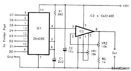
Where eight latching outputs are available, the Ferranti 2N426E probably represents the simplest means of providing an analog output. The figure shows the circuit diagram for a PC analog output port based on this chip. The full-scale output voltage is equal to the reference voltage fed to pin 5. This terminal can be fed from an external reference voltage of up to 3 V, but, in most cases, the built-in 2.55-V reference is perfectly adequate. The output voltage from IC1 (in volts) is equal to the value written to the printer port multiplied by 0.001. In most practical applications, this output-voltage range will have to be modified using an amplifier or an attenuator. In virtually all cases it will be a small amount of amplification that is required. This is the purpose of IC2, which also provides output buffering. The noninverting-mode amplifier IC2 can have its closed-loop voltage gain varied from unity to about 11 times by means of preset VR2.The maxinum output voltage of IC2 is about 2 V less than its supply potential (about 3 V) if it is powered from a 5-V supply. Therefore, maximum output voltages of more than 3 V require IC2 to be powered from a higher supply potential of up to about 30 V. This means using a separate supply for IC2 because the converter circuit must be powered from a 5-V supply. If preset VR1 is included, the best way to find the correct setting is to first write a low value to the port and adjust VR1 for the correct output voltage. Then write a high value to the port and adjust VR2 for the appropriate output voltage. Repeat this process a few times until no further adjustment is needed. If VE1 is omitted, write a value of 255 to the port and then adjust VR2 for the required maximum output voltage. Reasonable accuracy should then be obtained over the full range of output voltages.Using GW BASIC, it is just a matter of writing the values to the appropriate address using the OUT command. For example, OUT &H378,123 would write a value of 123 to a digital-to-analog converter connected to printer port LPT1. (View)
View full Circuit Diagram | Comments | Reading(676)
TIME_SHARED_TROUBLESHOOTER_SCOPE
Published:2009/7/12 20:58:00 Author:May
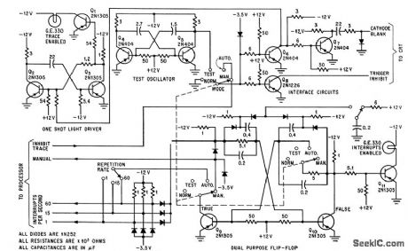
Oscilloscope modifications shown permit computer to control cro display for diagnosing trouble in faulty section of time-sharing comcomputer.-J. T. Quatse, Time-Shored Trouble-shooter Repairs Computers On-Line.Electronics,39:2,p97-101. (View)
View full Circuit Diagram | Comments | Reading(547)
GLITCH_FREE_CLIPPER
Published:2009/7/12 20:57:00 Author:May
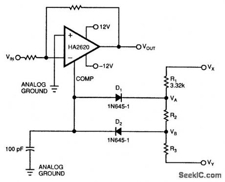

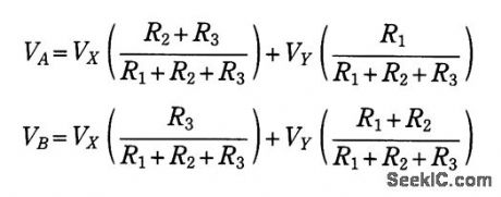
Adding a simple clamping circuit to a Harris 2620 high-speed op amp produces a glitch-free amplifier/ clipper. The op amp pin that controls the device's bandwidth is a high-impedance, isolated input. This pin also tracks the device's output voltage.Therefore, D1, D2, R1, R2, and R3 will clamp the amplifier's output voltage only when the amplifier's input voltage exceeds your clamping-voltage limits. VD is the diode drop of D1 or D2. The two clamp voltages, VA+VD and VB-VD, are:where VX and VY are the clamping circuit's bias voltages. Choosing R1 lets you determine the values of R2 and R3. Try a value for R1 around 3 kΩ.One example of this circuit had clamping voltages of ±3.7 V and exhibited THD below -75 dB for a sinusoidal, 30-kHz input signal. When the input signal increased beyond the ±3.7-V clamping voltage, the clipper symmetrically clamped the output voltage with no glitches in the waveform. (View)
View full Circuit Diagram | Comments | Reading(685)
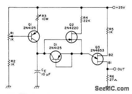
INHIBIT_DRIVER
Published:2009/7/12 20:56:00 Author:May
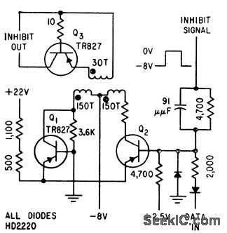
Used in coincident-current digital data buffer memory.-D. Haagens, Compact Memories Have Flexible Capacities, Electronics, 32:40, p50-53. (View)
View full Circuit Diagram | Comments | Reading(519)
10_h_FET
Published:2009/7/12 20:53:00 Author:May
Long duration timer gives adjustable delays up to 10 hours before turning Q3 on to give output voltage.-Circuits, 73 Magazine, Feb. 1974, p 101. (View)
View full Circuit Diagram | Comments | Reading(522)
MEMORY_STROBING_PULSE_GATE
Published:2009/7/12 20:53:00 Author:May


Used in generating precisely defined strobes for coincident-current memory. Uses drive-sampling core instead of clock signal to produce strobe at time when signal-to-noise ratio is highest.-A. H. Ashley and E. U. Cohler, Solving Noise Problems in Digitctl Computer Memories, Electronics, 33:13, p72-74. (View)
View full Circuit Diagram | Comments | Reading(494)
| Pages:194/471 At 20181182183184185186187188189190191192193194195196197198199200Under 20 |
Circuit Categories
power supply circuit
Amplifier Circuit
Basic Circuit
LED and Light Circuit
Sensor Circuit
Signal Processing
Electrical Equipment Circuit
Control Circuit
Remote Control Circuit
A/D-D/A Converter Circuit
Audio Circuit
Measuring and Test Circuit
Communication Circuit
Computer-Related Circuit
555 Circuit
Automotive Circuit
Repairing Circuit