
Index 197
CAPACITOR_STORAGE_FEEDBACK_BOXCAR
Published:2009/7/11 4:17:00 Author:May
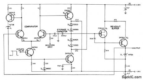
Improves accuracy of radar boxcar without sacrifice in speed, by using feedback principles to overcome instabilities in d-c offset voltages. Feedback forces boxcar output to equal input voltage during sampling, so intemal d-c offsets and instabilities Ionger than one storage interval are inconsequential. Box-car input goes to one terminal of difference amplifier, and boxcar output goes to other terminctl. Difference amplifer output is then used to control capacitor charge. By gating on difference ampliler during sampling interval, boxcctr output is made equcd to value of waveform at that time.-P. E. Harris and B. E. Simmons, DC Accuracy in a Fast Boxcar Circuit Via a Comparator, IEEE Transactions on Electronic Computers, June 1964, p 285-288. (View)
View full Circuit Diagram | Comments | Reading(871)
VOLTAGE_CONTROLLED_CURRENT_SINK
Published:2009/7/11 4:17:00 Author:May
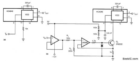
This circuit widens the linear frequency span of an HC4046 from one decade to nearly three decades. An LM358 is used as a constant-current sink to replace the frequency-determining resistor (10 kΩ) from pin 9 to ground. Pin 9 is held at a fixed 2.5 V for this application. (View)
View full Circuit Diagram | Comments | Reading(3240)
KEYER_WITH_MEMORY_1
Published:2009/7/11 4:04:00 Author:May
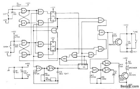
Features include dot and dash memory, gated clock, low standby and keydown currents, built-in sidetone oscillator with loudspeaker, and keying circuit for grid-block keyed transmitter. Will operate at least one year on 9-V transistor battery. Article describes circuit operation in detail. U1 is 4011 quad two-input NAND gate. U2 and U4 are 4081 quad two-input AND gates. U3 is 4013 dual D flip-flop. U5 is 4024 seven-stage binarv counter.U6 is 4071 quad two-input OR gate,U7 is 4001 quad two-input NOR gate,-E,A,Pfeiffer,MINIMOS-the Best Keyer Yet?,73 Magazine, Aug.1976,p 38-40 and 42-43. (View)
View full Circuit Diagram | Comments | Reading(812)
RECEIVING_DISTRIBUTOR
Published:2009/7/11 4:03:00 Author:May
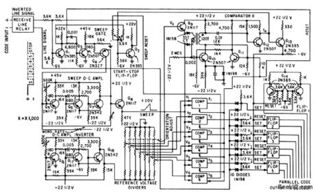
Converts tape-code input to 5-bit parallel code at five conventional flip-flops. Rising sweep voltage succes-sively triggers six comparator stages. If line signctl is positive at triggering time, flip-flop corresponding to triggered comparator is set to its one state. Used in high-speed electro-static printer in which each of 72 print heads has 35 print pins.-R,E,West,High-Speed Readout for Data Processing,Electronics,32:22,p83-85 (View)
View full Circuit Diagram | Comments | Reading(569)
CURVE_TRACER
Published:2009/7/11 4:02:00 Author:May
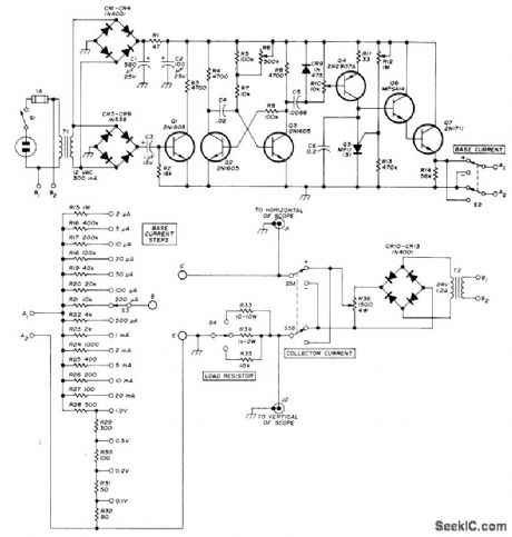

Displays on CRO a family of six collector characteristics for transistors and voltage/current characteristics of diodes, Circuit varies base voltage in discrete steps while sweeping collector voltage from zero to maximum at each step. Collector voltage is 120-Hz rectified sine wave from bridge rectifier CR10 CR13, varied by R36. S5 selects proper polarity. Base voltage steps are synchronized to 120-Hz colleetor voltage by adjusting R6 in mono MVBR Q2-Q3 driven by Q1. R10 adjusts voltage between steps. Programmable UJT Q5 resets staircase generator to zero. R12 adjusts gate voltage. Staircase voltage is coupled to bias resistors R15-R32 fortest transistor by Q6 and Q7, with bias polarity and value selected by S2 and S3. Connect device undertest to points B, C, and E. Connect points A1 and A2 together. R15-R35 should have 5% accuracy.-D. Wright, Transistor Curve Tracer, Ham Radio, July 1973, p 52-55. (View)
View full Circuit Diagram | Comments | Reading(3517)
STOPPING_PADDLE_BOUNCE
Published:2009/7/11 4:01:00 Author:May

Simple circuit prevents generation of erroneous dots by paddle contact bounce in keyers having dot memory. Uses 74121 mono MVBR and 7432 AND gate. Output of 74121 stays low if paddle is not in use or if dots or dashes are being sent. Release of dash paddle makes 74121 transmit high-level pulse to AND gate, long enough to block dot caused by bounce. Suitable only for keyers using +5 V.-B. Locher, Keyer Modifi-cation, Ham Radio, Aug. 1976, p 80. (View)
View full Circuit Diagram | Comments | Reading(1518)
KEYER_WITH_MEMORY
Published:2009/7/11 3:58:00 Author:May
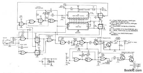
Low-drain CMOS circuit permits storage in RAM of message being keyed, for repeated later use by pushing button.Includes monitor, simple weight control, and both positive and negative keying outputs. Playback of stored message can be interrupted by closing either paddle contact. 1024-bit memory will hold two runs of alphabet, two sets of numbers, and several punctuation marks. Dot is stored as 1 followed.by 0; dash is three is followed by 0, Free-running clock ensures that spaces will be recorded.-C. B. Opal, The Micro-TO MeGsage Keyer, QST, Feb. 1978, p 11-14. (View)
View full Circuit Diagram | Comments | Reading(1042)
CODE_REGENERATOR
Published:2009/7/11 3:55:00 Author:May

Converts noisy CW output of receiver into TTL 1 s and 0s for driving automatic Morse-code printer. Clipper U1A and 800-Hz active bandpass filter U1B feed injection-locked 800-Hz phase-shift oscillator U3 (National LM7401CN or Motorola HEP-C6052P).U1 is LM1458N or MC1458P. U2 uses part of LM709CN or HEP-C6103P as matched pair of 7-V back-to-back zener diodes. Diode detector D1 has time constant of about 5 ms, which is short enough for highest Morse-code speeds. Detector feeds LM311N or MLM311P1 voltage comparator U4 which can drive TTL or DTL directly, National LM380N audio amplifier U5 allows CW signal to drive loudspeaker directly.-H. Olson, CW Regen erator/Processor, 73 Magazine, July 1976, p 80-82. (View)
View full Circuit Diagram | Comments | Reading(1095)
UNIVERSAL_KEYBOARD_ENCODER
Published:2009/7/11 3:52:00 Author:May

Harris HD-0165 keyboard encoders are combined with three read-only memories wired in parallel to generate universal code that can be translated to desired output code by using suitable electric programming of ROMs. Key-to-encoder wiring is arbitrary as long as each key operation produces unique 6-bit output code from encoders.One ROM is programmed to contain all 64 output words for unshifted mode, second for shifted mode, and third ROM contains all words for control mode.- Linear & Data Acquisition Products, Harris Semiconductor, Melbourne, FL, Vol. 1, 1977, p 7-2-7-B (Application Note 204). (View)
View full Circuit Diagram | Comments | Reading(2404)
CHOPPER_TRANSISTORS_SIMULATE_SPDTSWITCH
Published:2009/7/11 3:49:00 Author:May
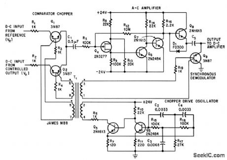


Comporator chopper senses difference between reference voltage and control signal while drowing very little current from reference. Sine-wave drive frequency is determined by C2 and C3, which should have 2 to 1 ratio.-J.S.Mac Dougall,Servo Comparator Amplifier Handles High Voltages,Electronics,37:22.p75-76 (View)
View full Circuit Diagram | Comments | Reading(751)
PULSE_ANALYZER
Published:2009/7/11 3:43:00 Author:May
Either positive or negative pulses equal to or greater than adjustable threshold voltage operate relay ,thus measuring pulse height of either poktrity. Responds to pulse widths as narrow as 50 nsec.Q1 responds to positive pulses, and Q2 to negoiive pulses.-O.B.laug,Pulse Voltage Comparator Measures Height of Positive or Negative Pulses, Electronics, 34:36, p70-71. (View)
View full Circuit Diagram | Comments | Reading(825)
SCANNER_VOICE_SQUELCH
Published:2009/7/11 3:42:00 Author:May

This circuit detects the presence of audio (voice) on the output of a scanner. If the scanner stops on a dead carrier or noise, the circuit mutes the speaker to avoid annoying noise.U1 amplifies speech and drives rectifier D1/D2 and switch Q1. Comparator U3 drives speaker switch Q1 and indicator LED1. Q2 completes the speaker path to ground. U2 is an audio amplifier to drive the speaker. R3 is a volume control. PL1 connects to the scanner speaker or to the headphone jack. (View)
View full Circuit Diagram | Comments | Reading(1182)
SIMPLE_VOX
Published:2009/7/11 3:39:00 Author:May
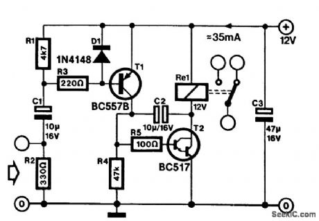
A VOX is a voice-operated switch that is often used as a substitute for the press-to-talk switch on a microphone. This VOX can be connected to almost any audio equipment that has a socket for an external loudspeaker. The actuation threshold is set by the volume control on the AF amplifier that drives the VOX.The (loudspeaker) signal across R2 is capacitively fed to the base of T1. Resistor R3 limits the base current of this transistor when the input voltage exceeds 600 mV. Diode D1 blocks the positive excursions of the input signal, so that Veb cannot become more negative than about 0.6 V.The output relay is driven by Darlington T2. Resistor R4 keeps the relay disabled when T1 is off. The value of bipolar capacitor C2 allows it to serve as a ripple filter in conjunction with T2. Resistor R5 limits the base current of T2 to a safe level.The switching threshold of the VOX is about 600 mV across R2. The maximum input voltage is deter-mined by the maximum permissible dissipation of R2 and R3. As a general rule, the input voltage should not exceed 40 Vpp. The current drawn by the VOX is mainly the sum of the currents through the relay coil and through R5. The resistor can carry up to 100 mA when the VOX is overdriven. (View)
View full Circuit Diagram | Comments | Reading(3055)
CHARACTER_READER
Published:2009/7/11 3:35:00 Author:May
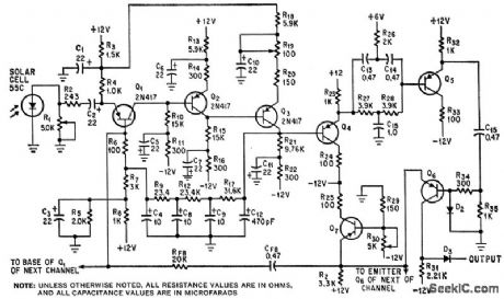


Circuit shows one channel of solar-cell sigmctl amplifier and section of switching bolck for experimental character recognition system.-P.H. Howard, Feedback System Detects 1% Amplitude Difference,Electronics,38:10,p68-70 (View)
View full Circuit Diagram | Comments | Reading(676)
128_BIT_CODE_STORE
Published:2009/7/11 3:30:00 Author:May
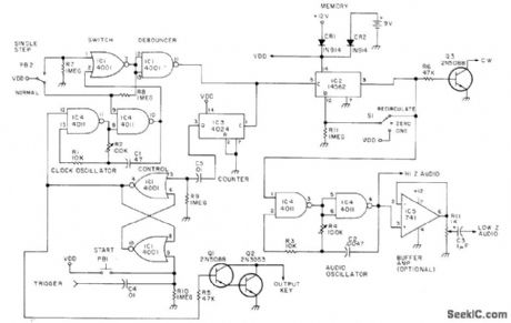
Draws almost no power, can be used on RTTY as well as CW, and can be reprogrammed in less than 1 min. Built around Motorola MC14562CP 128-bit shift register. Combination of 1 (high level) and 0 (low level) bits forming identifier message is fed into of shift register and leave only 0s. Now, set S1 to desired first 1 or 0, push switch PB2 once, and repeat for rest of coded identifier. Set S1 to RECIRCULATE push PB1 to cycle back to starting point, and unit is ready for use. If debouncer is not effective, move its wire from IC1-11 to IC4-10. Easier-to-get altemate values for C1 and R2 are 0.05 μF and 1 megohm.-C. W. Andreasen, Programmable CW ID Unit, 73 Magazine, Oct.1976, p 52-53. (View)
View full Circuit Diagram | Comments | Reading(880)
CW_FILTER_1
Published:2009/7/11 3:28:00 Author:May
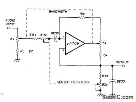
Variable-bandwidth variable-frequency audio filter can be tuned to center frequency anywhere in range from 300 to 3000 Hz.Bandwidth can be as narrow as 50 Hz, which is about 3 times theoretical minimum of is Hz for 50-bit words and Morse code at 25 WPM. Performance can be improved over entire fre-quency range by using 741 opamp.-R. Skelton, Comments, Ham Radio, June 1975, p 56-57. (View)
View full Circuit Diagram | Comments | Reading(902)
ELECTRONIC_CHRONOMETER
Published:2009/7/11 3:24:00 Author:May
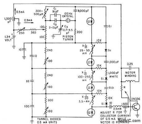
Trimmers permit adjusting timing by a few seconds per year.Major error is due to aging of quartz crystal,Tunnel diodes divide 100-kc crystal frequency by 2,000 to give 50-cps output for driving motor of clock.-R. L. Watters, Tunnel Diodes Control Quartz-Crystal Chronometer, Electronics, 34:39, p129-131. (View)
View full Circuit Diagram | Comments | Reading(655)
SHORT_PROTECTION_AND_SHUTDOWN_CIRCUIT
Published:2009/7/17 2:36:00 Author:Jessie
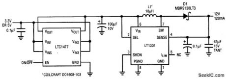
An LT1301 is used in the figure to boost a 3.3-V or 5-V input to 12 V, as for Vpp for flash memory. Although the LT1301 features a shutdown control, the input supply can still feed through to the output through L1 and D1. Similarly, a short circuit on the output could drag down the input supply. With the addition of the LTC1477, the circuit furnishes 100-percent load shutdown and output short-circuit protection. (View)
View full Circuit Diagram | Comments | Reading(657)
FREQUENCY_SWEEPER
Published:2009/7/11 3:16:00 Author:May
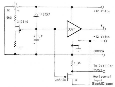
Sawtooth output of UJT varies sinusoidal output frequency of Optical Electronics 3370 voltage-to-frequency transducer, as required for checking frequency response of active and passive networks. R1 determines sweep width. Center frequency of sweep output can be changed by adding voltage to sawtooth or adjusting 3370. Sweep speed can be increased by reducing value of 1-μF tantalum capacitor.- Sweep Generator Using a Voltage-to-Frequency Transducer, Optical Electronics, Tucson, AZ, Application Tip 10059. (View)
View full Circuit Diagram | Comments | Reading(920)
200_BIT_MEMORY
Published:2009/7/11 3:15:00 Author:May
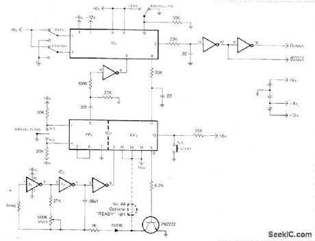
Drawback of volatile codestoring memory is offset by low cost and com parative ease of programming. IC1 is Signetics 2511D MOS dual 200-bit shift register whose digital levels are shifted one position for each dock pulse. Inverters I1 and I2 of CMOS hex inverter IC3 form variable-frequency gated square-wave clock oscillator controlled by state of flip-flop FF2 in 74C74 CM0S dual D flip-flop. Shift register must first be cleared by setting DATA and CONTROL switches to ground and RECIRCULATE switch to hold, then pressing START button (with speed control set fast) until register is full of zeros, Release START button and switch control to +6 V for about 10 s. Now set CONTROL to ground and start programming. To enter dah, switch manual clock through three complete up-center/down-center cycles, switch data line to ground, and cycle manual clock through one cycle to insert space into memory. To enter dit, switch manual clock through only one up/down cycle. Continue until entire message is entered in register, switch to RECIRCULATE, and push START switch. Message will now be sent in perfect code at any desired speed.-B. P. Vandenberg, An Inexpensive Memory Keyerfor Contests, CQ, May 1976, p 50-51. (View)
View full Circuit Diagram | Comments | Reading(623)
| Pages:197/471 At 20181182183184185186187188189190191192193194195196197198199200Under 20 |
Circuit Categories
power supply circuit
Amplifier Circuit
Basic Circuit
LED and Light Circuit
Sensor Circuit
Signal Processing
Electrical Equipment Circuit
Control Circuit
Remote Control Circuit
A/D-D/A Converter Circuit
Audio Circuit
Measuring and Test Circuit
Communication Circuit
Computer-Related Circuit
555 Circuit
Automotive Circuit
Repairing Circuit