
Index 196
BINAURAL_SYNTHESIZER_FOR_CW
Published:2009/7/11 5:06:00 Author:May
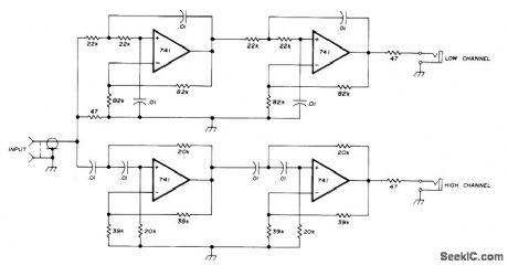
Provides two channels for feeding stereo phones or two loudspeakers. When interference occurs a few hundred hertz from desired frequency, receiver is tuned so desired signal appears to be midway between loudspeakers, leaving interfering signals at right or left. Left or low channel has low-pass active filter and right or high channel has high-pass filter, with crossover at 750 Hz. Synthesizer is designed for low-impedance drive, as from loudspeaker output of receiver. Resistors in output channels prevent oscillation when 8-ohm phones or loudspeakers are directly connected to outputs. Opamps will drive 2000-ohm phones with ample volume and give moderate volume levels with 8-ohm loads.-D. E. Hildreth, Synthesizer for Binaural CW Reception, Ham Radio, Nov. 1975, p 46-48 (View)
View full Circuit Diagram | Comments | Reading(1464)
CW_SIDETONE
Published:2009/7/11 5:05:00 Author:May
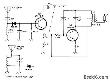
Audio sidetone oscillator serves for monitoring CW keying. Changes in transmitter operating frequency do not affect sidetone circuit. Hartley AF oscillator Q2 is turned on by diode rectifier and DC amplifier Q1.Antenna coupling shown is adequate from 160 through 10 meters. For VHF use on 6 and 2 meters, small tuned circuit and pickup antenna are usually required to get enough RF input for monitor. Audio pitch is adjusted by changing value of C1.-J. Fisk, Circuits and Techniques, Ham Radio, June 1976, p 48-52. (View)
View full Circuit Diagram | Comments | Reading(2905)
PASSIVE_CW_FILTER
Published:2009/7/11 5:05:00 Author:May

Uses inexpensive 88-mH toroids to give very sharp 35-Hz bandwidth at 3 dB down. Filter has high insertion loss. Keyed waveshape has slow rise and fall, so CW signals have pronounced ringing that may be objec-tionable.-A. F. Stahler, An Experimental Com-parison of CW Audio Filters, 73 Magazine, July 1973, p 65-70. (View)
View full Circuit Diagram | Comments | Reading(1604)
CODE_PRACTICE
Published:2009/7/11 5:03:00 Author:May
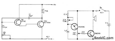
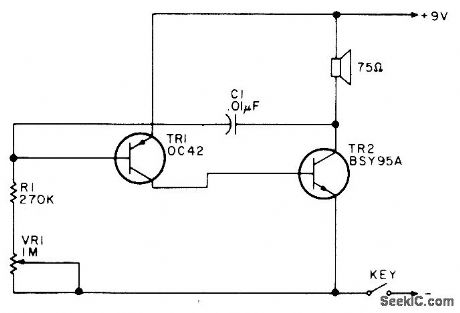
Simple AF oscillator drives loudspeaker for producing audio tone when key in negative supply lead is closed. Adjust VR1 for most pleasing tone.-Circuits, 73 Magazine, July 1975, p 154. (View)
View full Circuit Diagram | Comments | Reading(790)
VLF_CONVERTER
Published:2009/7/11 5:03:00 Author:May
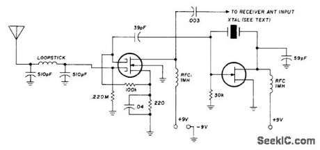
Uses low-pass filter instead of usual tuned circuit, so only associated receiver need be tuned. Measured threshold sensitivity is about 20 μv. Transistors used in dual-gate MOSFET mixer and FET oscillator are not critical. Crystal can be any frequency compatible with tuning range of receiver used. With 3.5-MHz crystal, 3.5 MHz on receiver dial corresponds to 0 kHz and 3.6 MHz to 100 kHz.-R. N. Coan, VLF Converter, Ham Radio, July 1976, p69. (View)
View full Circuit Diagram | Comments | Reading(0)
220_MHz_TO_28_MHz
Published:2009/7/11 5:00:00 Author:May
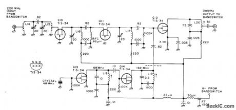
Contains bandpass filter, grounded-grid RF amplifier stages Q10-Q11, mixer Q12, and crystal oscillator Q13-Q14. Developed for use in all-band double-conversion superheterodyne receiver for AM narrow-band FM, CW, and SSB operation. Supply is 13.6 V regulated. Article gives all circuits of receiver. -D. M. Eisenberg, Build This All-Band VHF Receiver, 73 Magazine, Jan. 1975, p 105-112. (View)
View full Circuit Diagram | Comments | Reading(2322)
144_MHz_T0_28_MHz
Published:2009/7/11 4:58:00 Author:May
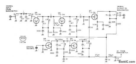
144 MHz T0 28 MHz-Contains bandpass filter, grounded-grid RF amplifier stages Q5- Q6, mixer Q7, and crystal oscillator Q8-Q9. Developed for use in all-band double- conversion superheterodyne receiver for AM, narrow-band FM, CW, and SSB operation. Supply is 13.6 V regulated. Article gives all circuits of receiver-D. M. Eisen. berg, Build This All-Band VHF Receiver, 73 Magazine, Jan. 1975, p 105-112. (View)
View full Circuit Diagram | Comments | Reading(3590)
KEYER_WITH_MEMORY_2
Published:2009/7/11 4:57:00 Author:May
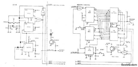
Clock Z1 is NE555 timergiving keying speed range of 5 to 35 WPM.Flip-flops Z2A and Z2B count clock pulses to provide self-completing dits and dahs with spaces. Z4 and Z5 are 4-bit binary counters used for addressing static 256 × 1 bit RAM. To program keyer, switch to write, hit START button, and feed in message on keyer paddle. To send message back, switch to read and hit START again. To clear address counter if error is made, or for changing message, hit RESET switch and start over again.-D. W. Sewhuk, Contest Special Kever, 73 Magazine, Feb. 1977, p 38. (View)
View full Circuit Diagram | Comments | Reading(630)
50_MHz_TO_28_MHz
Published:2009/7/11 4:57:00 Author:May
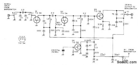
Contains bandpass filter, two grounded-grid RF amplifier stages Q1-Q2, mixer Q3, and crystal oscillator Q4. Developed for use in all-band double-conversion superheterodyne receiver for AM narrow-band FM, CW, and SSB operation. Supply is 13.6 V regulated, Article gives all circuits of receiver, -D. M. Eisenberg,Build This All-Band VHF ReceiVer,73 Magazine,Jan,1975,p 105-112. (View)
View full Circuit Diagram | Comments | Reading(1588)
1_3_DOT_DASH_KEYER
Published:2009/7/11 4:55:00 Author:May
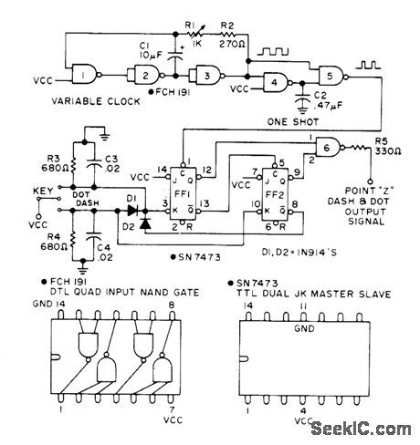
Gives accurate 1 :3 dotdash ratio at any desired keying speed, with self-completing characters. NAND gates 1, 2, and 3 of first FCH191 form variable-frequency square-wave oscillator, with C1, R1, and R2 determining frequency. With values shown, frequency is adjustable from about 150 to 1500 Hz, equivalent to code speed range of about 4 to 40 WPM. NAND gates 4 and 5 form mono MVBR. Flip-flops FF1 and FF2 are SN7473 TTL JK master-slave, acting with D1, D2, and NAND gate 6 to generate dots and dashes.-H. P. Fischer, Versatile IC Keyer, 73 Magazine, Sept. 1973, p 69-71. (View)
View full Circuit Diagram | Comments | Reading(932)
COCKCROFT_WALTON_CASCADED_VOLTAGE_DOUBLER
Published:2009/7/11 4:55:00 Author:May
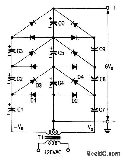
A center-tapped transformer of secondaryvoltage.Two VS can be used to power a voltage multiplier. For higher voltages,simply add more sections. (View)
View full Circuit Diagram | Comments | Reading(1101)
20_KC_CHOPPER
Published:2009/7/11 4:54:00 Author:May
Square-loop-core oscilkttor drives chopper at up to 20 kc for continuously monitoring two d-c voltages.-J. W.Higginbotham And H. H. Douglass, Voltage Compctrator with High-Speed Switches, Electronics, 32:5, p56-58. (View)
View full Circuit Diagram | Comments | Reading(615)
VOLTAGE_DOUBLERS
Published:2009/7/11 4:52:00 Author:May
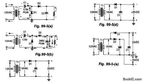
During the first half-cycle (Fig. 99-5(a)), D1 conducts, D2 cuts off, C1 charges to 170 V peak, and C2 discharges through RL For the second half-cycle (Fig. 99-5(b)), the input polarity is reversed, and both the input and C1 are in series, which produces 340 V (peak). Now, D1 cuts off, while D2 conducts, and the current divides between C2 and RL; the cycle then repeats. Two Half-Wave Rectifiers, one with a positive output (Fig. 99-5(c)) and one negative (Fig. 99-5(d)), combine to make a full-wave voltage doubler (Fig. 99-5(e)). (View)
View full Circuit Diagram | Comments | Reading(762)
DYNAMIC_LOAD
Published:2009/7/11 4:37:00 Author:May
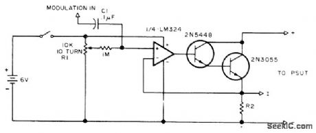
R1 sets load current drawn from power supply under test to desired value, after R2 is chosen to give about 1-V output at maximum load currentto be drawn from power supply under test (PSUT). Modulation input to C1 is obtained from external pulse generator, and selves to make load current increase and decrease over small range.-R. Tenny, Power Supply Testing, 73 Magazine, July 1976, p 112.114 and116-117. (View)
View full Circuit Diagram | Comments | Reading(886)
CW_STEREO_FILTER
Published:2009/7/11 4:35:00 Author:May
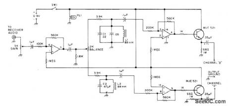
Developed to enhance ability to read CW despite heavy contest traffic or other QRM. Two high-Q filters, one at each end of 400-Hz CW filter in receiver, create separate audio channels to give effect of stereo.Transistors at outputs of channels provide extra current gain for driving low-impedance stereo headphones. CW signal at 800 Hz then appears to comefrom left, 1200-Hz signal from right, and in between frequencies at various azimuth angles. Illusion of direction makes it easier for operator to concentrate on desired signal in presonce of others having slightly different frequencies. L1 and C1 form filter for 1200-Hz channel, while L2 and C2 form 800-Hz filter for other channel.-R. L. Anderson, Stereo-a New Type of CW Filter, 73 Magazine, March 1976, p 48-50. (View)
View full Circuit Diagram | Comments | Reading(920)
VOLTAGE_MULTIPLIER
Published:2009/7/11 4:35:00 Author:May
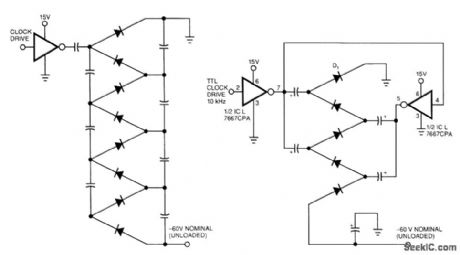
Figure 99-l(a)'s circuit exhibits a high-output impedance as a result of the small effective capacitance of the series-connected capacitors, and it exhibits considerable voltage loss due to all of the diode drops. Further, this circuit requires 2n diodes and 2n capacitors to produce a dc output voltage approximately n times the rail voltage.Figure 99-1(b)'s circuit multiplies more effectively using fewer diodes and capacitors. The parallel arrangement of the capacitors lets you use smaller capacitors than those required in Fig. 99-1(a). Alternatively, when using the same capacitor values of Fig. 99-1(a), the output impedance will be lower.Whereas the clock source directly drives only one of the two strings of capacitors in Fig. 99-1(a), Fig. 99-1(b)'s clock drives both strings with opposite phases. This drive scheme doubles the voltage per stage of two diodes. A final diode is necessary to pick off the dc output voltage because both strings of capacitors now carry the p-p ac input-voltage waveform. The ICL7667 dual-FET driver accepts a TTL drive swing and provides a low-impedance push-pull drive to the diode string. This low impedance is particularly helpful when using a long string to raise output voltage to more than 100 V, starting from a low rail voltage. (View)
View full Circuit Diagram | Comments | Reading(1156)
CW_IDENTIFIER
Published:2009/7/11 4:34:00 Author:May
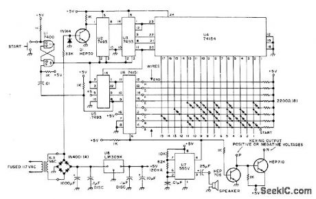
Circuit automatically gener ates call Ietters for FCC-required code identification for FM repeaters and RTTY, when started by pushbutton or by pulse from other equip ment. Audio output can be fed to loudspeaker as monitor or used to modulate FM repeater.Circuit shown is programmed for DE K4EEU by installing diodes at locations where tone is wanted on matrix. Article gives construction and programming details.-B. Kelley, A Super Cheapo CW IDer, 73 Magazine, Dec. 1976, p 46-48. (View)
View full Circuit Diagram | Comments | Reading(2100)
AUTOMATIC_HI_ON_HORN
Published:2009/7/11 4:29:00 Author:May
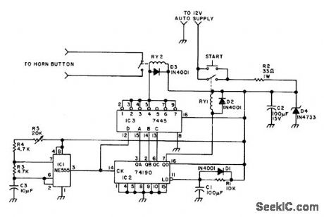
Pressing start button of circuit momentarily makes it send letters H1 in Morse code on automobile horn, as friendly signal to another ham on road. Uses NE555 timer as oscillator, acting with counter 102, decoder IC3, power-supply latch, and regulator. Space betweqn four dots of H and two dots of I is achieved by not using pin 5 of decoder. RY1 should pull in at 5 V and 16 mA maximum,while RY2 should pull in at 5V and 80 mA maximum and have contacts for switching 0.5-A inductive load of horn.-J. F. Reid, Sending HI, 73 Magazine, May 1977, p 90. (View)
View full Circuit Diagram | Comments | Reading(1063)
OUASI_BREAK_IN
Published:2009/7/11 4:28:00 Author:May
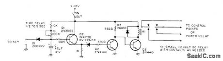
Amateur station stays in receive mode until operator starts to send code. Tapping on key makes transmitter switch into transmit mode and stay there after last character is sent, for delay of several seconds (determined by R1) before transmitter is deenergized, Developed for use with cathode-keyed transmitters,-F,E,Hinkle,Jr,KOX for CW 73 Magazine, Feb 1975,p 129-130. (View)
View full Circuit Diagram | Comments | Reading(635)
AF_SIGNALTRACER
Published:2009/7/11 4:23:00 Author:May
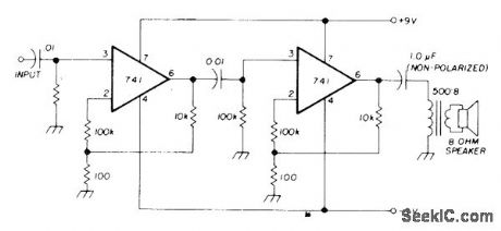
High-gain audio amplifier with loudspeaker output serves for troubleshooting AF stages. With normal input to amplifier under test, presence of AF signal is tested in each stage in turn. If AF signal appears at input of stage but not at output, that stage has a defect. Signal source may also be signal injector having broadband output from audio through VHF.-M. James, Basic Troubleshooting, Ham Fladio, Jan. 1976, p 54-57. (View)
View full Circuit Diagram | Comments | Reading(632)
| Pages:196/471 At 20181182183184185186187188189190191192193194195196197198199200Under 20 |
Circuit Categories
power supply circuit
Amplifier Circuit
Basic Circuit
LED and Light Circuit
Sensor Circuit
Signal Processing
Electrical Equipment Circuit
Control Circuit
Remote Control Circuit
A/D-D/A Converter Circuit
Audio Circuit
Measuring and Test Circuit
Communication Circuit
Computer-Related Circuit
555 Circuit
Automotive Circuit
Repairing Circuit