
Index 198
PLL_CODE_REGENERATOR
Published:2009/7/11 3:13:00 Author:May
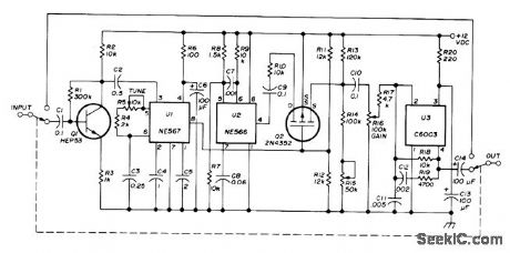
Permits comfortable listening to CW signals deeply embedded in noise, hash, and interference, by detecting one particular CW transmission and keying independent oscillator with its signal. Consists of signal amplifier Q1, narrow-band PLL frequency detector and trigger U1, PLL function generator U2, gate Q2, and AF output amplifier U3. In absence of triggering signal, output pin 8 of U1 presents high impedance to ground. With trig-gering frequency, output presents low impedance to ground. Oscillator U2 is gated by un through Q2.-C. R. Lewartand R. S. Libenschek, CW Regenerator for Interference-Free Communications, Ham Radio, April 1974, p 54-56. (View)
View full Circuit Diagram | Comments | Reading(1072)
SYNC_SEPARATOR
Published:2009/7/11 3:08:00 Author:May
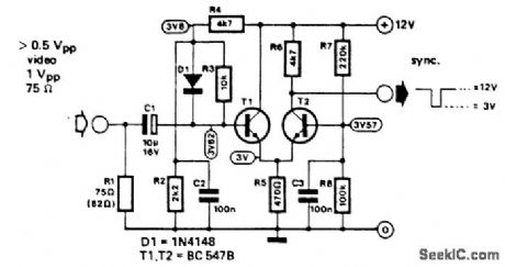
This circuit separates the synch from the composite video signal.It uses a two-transistor comparator.Output is 9 VPP a 0.5-VPP (minimum) video input signal. (View)
View full Circuit Diagram | Comments | Reading(4951)
PROM_CW_IDENTIFIER
Published:2009/7/11 3:07:00 Author:May
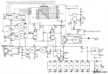
Call letters stored in 8223 PR0M U3 drive 74151 multiplexer/data selector U4 for keying NE555 audio oscillator U5 which feeds transmitter mike input through RA.Timed holdoff keeps identifier from being rekeyed within spedfied time period, with reiden.tifying at end of period. Article covers operation of circuit and gives construction and programming details,ID with a PROM,73 Magazine, Nov,1976,p 90-92. (View)
View full Circuit Diagram | Comments | Reading(1482)
REGENERATIVE_CW_FILTER
Published:2009/7/11 3:06:00 Author:May
Can be added between product detector and volume control of SSB receiver or transceiver that does not have CW filter. Just before oscillation oceurs, gain becomes extremely high with very narrow bandpass. Regeneration and bandpass can be adjusted as required. Filter typically has 40-Hz bandwidth centered on 800 Hz.-R. A. Yoemans, Further Enhancing the Yaesu FTDX-560 Transceiver, CQ, July 1972, p 16-18 and 20-22. (View)
View full Circuit Diagram | Comments | Reading(1575)
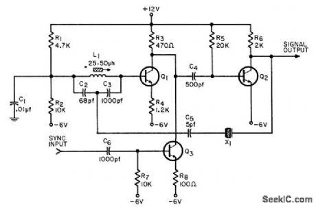
THREE_PHASE_1O_MC_CLOCK
Published:2009/7/11 3:06:00 Author:May
Used in digital computer circuit testing when recirculcttion of pulses and pulse regeneration and shaping are required. Delay line provides required impedance match.-R. W. Buchanan and B.Kautz, Dynamic Testing of Computer Building Blocks, Electronics, 32:33, p66-68. (View)
View full Circuit Diagram | Comments | Reading(587)
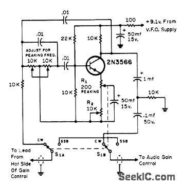
CW_FILTER
Published:2009/7/11 3:05:00 Author:May
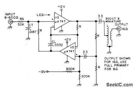
Simple single-section parallel-tuned active filter uses negative-impedance converter or gyrator to replace hard-to-get inductor of passive code filter. Capacitor CL is gyrated from 0.0332 ptF to effective inductance of 1.87 H. Filter has 6-dB gain at resonance and essentially zero output impedance. Bandpass is 85 Hz centered at about 865 Hz. Uses single -12 V supply. Resistors R are 7.5K, matched to about 2%.-N. Sipkes, Build This CW Filter, 73 Mag-azine, June 1977, p 55. (View)
View full Circuit Diagram | Comments | Reading(984)
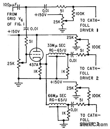
SYNCHRONIZING_33_MC_CLOCK_TO_300_PPS_TRIGGER
Published:2009/7/11 2:56:00 Author:May
Synchronizes crystal-controlled tran of of 3.3-Mc clock pulses to unrelaled sync trigger having nominal repetition rate of 300 pulses per second, to provide constant delay between end of sync pulse and first clock pulse.-P. Danzer, Synchronized, Crystal-Controlled Oscillcator, EEE, 12:5, p90. (View)
View full Circuit Diagram | Comments | Reading(562)
FAST_BREAK_IN
Published:2009/7/11 2:55:00 Author:May
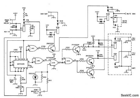
Permits operator to hear signals even between dots while calling DX station, so call can be stopped if DX station answers someone else. Timing circuit ensures that transmitter is not producing power when relays open, permitting use of small high-speed relays. K1-K4 are common reed relays. K5 should have contacts rated for 300 VAC at 500 mA.-A. Pluess, A Fast aSk System Using Reed Relays, QST, Dec. 1976, p 11-12. (View)
View full Circuit Diagram | Comments | Reading(635)
FOUR_PHASE_12_MC_CLOCK
Published:2009/7/11 2:48:00 Author:May
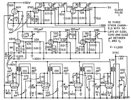
To minimize litter of synchronizing signals, fundomentcd frequency is chosen at one-eighth of dock rate or 1.5 Mc. Oscillator output is fed through two doubler stages and split into three channels, each having additional doubler followed by power amplifier, to provide low output impedance at any reasonable power level.-G.O. Olson, Design of High-Frequency Clock Pulse Generators, Electronics, 32:35, p56-57. (View)
View full Circuit Diagram | Comments | Reading(589)
VR_TUBE_CHECKER
Published:2009/7/11 2:47:00 Author:May
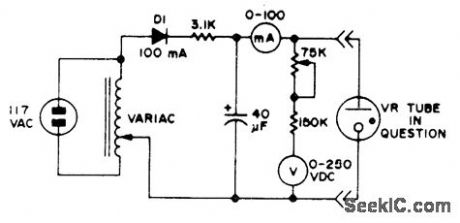
Increase output voltage of Variac gradually until VR tube fires, then read milliammeter and voltmeter. Good tubes will fire at their rated voltage and current values.-Circuits, 73 Magazine, May1977,p31. (View)
View full Circuit Diagram | Comments | Reading(942)
DIODE_CHECKER
Published:2009/7/11 2:46:00 Author:May
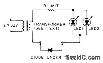
Requires only one resistor, two LEDs, and any small power transformer providing 3 to 25 VAC. If diode under test is open, neither LED lights, lf diode is shorted, LED1 lights on one half-cycle and LED2 on other half-cycle, so both appear lit continuously. If diode is good, LED1 will light if anode of diode is toward transformer, and LED2 will light for other polarity of diode. Choose resistor to limit current through LEDs to about 10 mA.-M. D. Kitchens, Ultra Simple Diode Checker, 73 Magazine, Oct. 1977, p 44-46. (View)
View full Circuit Diagram | Comments | Reading(583)
POCKET_SIZE_CRYSTAL_CHECKER
Published:2009/7/11 2:44:00 Author:May
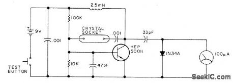
Providesquick check of condition when shopping for used or surplus crystals Meter gives steady indieation at about half scale when test button is pushed, if crystal is oscillating properly.-Circults,73 Magazine, April 1977, p 164. (View)
View full Circuit Diagram | Comments | Reading(701)
PARLLEL_TO_SERIAL_CONVERSION
Published:2009/7/11 2:37:00 Author:May
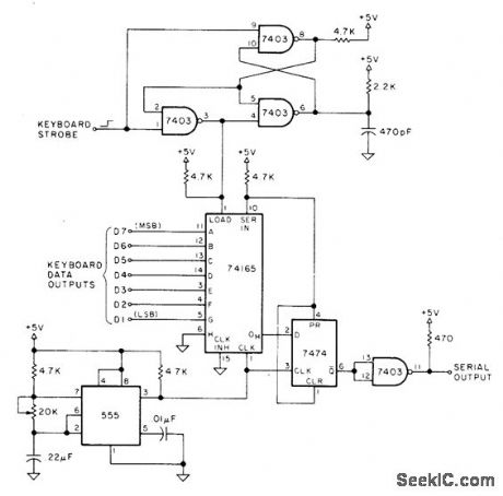
Can be used as interface between parallel outputs of keyboard and serial input port of microprocessor. Keyboard output data is fed to 74165 shift register, with eighth input tied low. 7403 gates are connected as mono MVBR for converting keyboard strobe to narrow pulse for loading shfft register. Fourth gate in package serves as output buffer. 555 timer forms clock adjustable from 150 to 1400 Hz, to allow operational standard baud rates of 150, 300, 600, or 1200.-F. J.Greeb, Who Needs a UART?, Kilobaud, Aug.1978, p 108. (View)
View full Circuit Diagram | Comments | Reading(2677)
PHASE_SYNCHRONIZER
Published:2009/7/11 2:33:00 Author:May
Used to synchronize 2,500-cps local time standard with that of transmitting end of wire-line system. When zero crossings of pulses do not coincide, error signal is produced which, after amplification, is applied to motor that rotates phase shifter until there is phase synchronization between local clock and incoming information.This insures sampling of recovered information at middle of incoming bit.-J.L.Hollis, Sending Digital Data Over Narrow-Band Lines, Electronics, 32:23, p72-74. (View)
View full Circuit Diagram | Comments | Reading(850)
RGB_NTSC_CONVERTER
Published:2009/7/11 2:31:00 Author:May
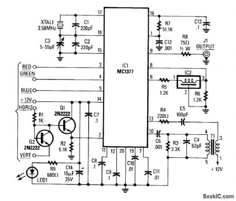
Using a Motorola MC1377, this circuit produces NTSC video from an RGB source. Components are not critical, except for R7 and CB, which should be 1% and 2% tolerance. respectively. (View)
View full Circuit Diagram | Comments | Reading(3908)
CQ_CALL_SYNTHESIZER
Published:2009/7/11 2:31:00 Author:May
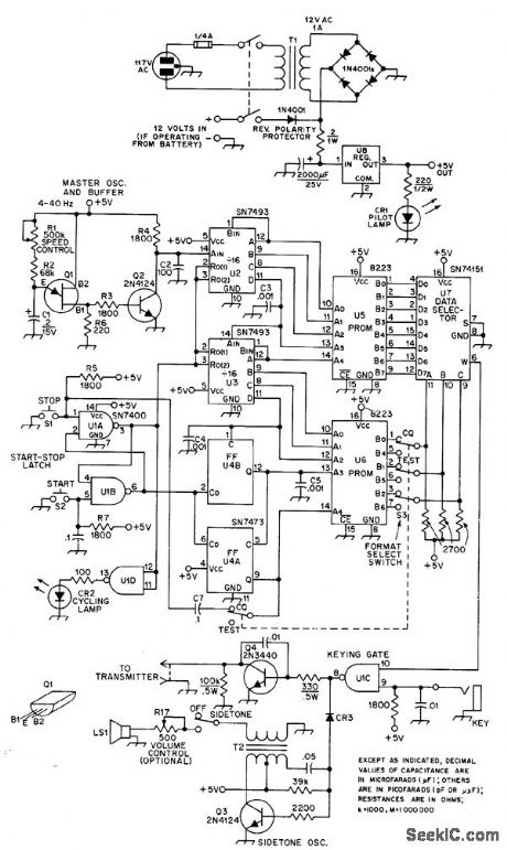
Uses only two Signetics 8223 256-bit PROMs for storing up to 2048 bits of code information, for automatic generation of Morse-code CQ calls, test messages, and other frequently used messages. Repeated words are stored in only one location and selected as needed, to quadruple capacity of memory. PROMs can be programmed in field or custom-programmed by manufacturer.Speed and timing of code characters are deter.mined by UJT oscillator 01, variablefrom about 4 to 40 Hz or 5 to 50 WPM. CR1 and CR2 are Archer (Radio Shack) 276-042 orequivalent. CR3 is 1N34A, 1N270, or equivalent germanium. Q1 is Motorola MU4891 or equivalent. Article describes circuit operation and programming in detail-J. Pollock, A Digital Morse Code Syn thesizer, QST, Feb. 1976, p 37-41. (View)
View full Circuit Diagram | Comments | Reading(942)
TRANSISTOR_CURVE_TRACER
Published:2009/7/11 2:31:00 Author:May
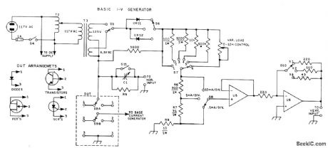
When fed with staircase waveform of base-culrent generator, circuit generates series of current-voltage (I-V) curves as function of base current, for transistors and other three-terminal semiconductor devices. Cathodefollower U5 and inverting controlled-gain amplifier U6 can be eliminated if correct sense of current indication is not essential. S11 switches multiplier R9 in and out; R9 is 18 megohms (about 9 times input resistance of CRO). C1 is 7-13 pF mica trimmer. Diodes are 1N4822. U5 and U6 are Fairchild 741. T2 is Knight 54A3800 or equivalent variable autotransformer rated 1 A. T3 is Knight 54A141O or equivalent power transformer with 125-V 15-mA and 6.3-V 0.6-A secondaries.-R. P. Ulrich, A Semiconductor Curve Tracer for the Amateur, QST, Aug. 1971, p 24-28. (View)
View full Circuit Diagram | Comments | Reading(4539)
_VIDEO_A_D-D_A_CONVERTER
Published:2009/7/11 2:29:00 Author:May

This circuit is useful for digital video experiments and for interfacing video with a computer that has a TDA8708 (Philips). The A/D converter provides 8-bit digitized video to k23 socket and k21 socket. A TDA8702 (Philips) D/A converter recovers analog video. IC3 is a 1- to 5-ms delay line (1505) to delay clock pulses in 1-ms steps to the DiA converter. Clock speeds can be up to 30 MHz. Three video inputs are provided for three analog channels (e.g., R, G, B video). (View)
View full Circuit Diagram | Comments | Reading(1953)
SETTING_CLOCK_TO_WWV
Published:2009/7/11 2:27:00 Author:May
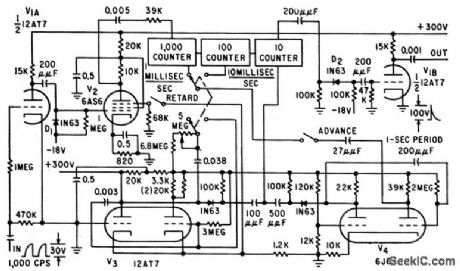
Locally genemted pulses can be easily synchronized with pulses from WWV to see clocks associated with frequency standard. Changes in period of pulses from counter-type frequency dividers are made with precision vernier. Any 10-stable divider can be used in counler circuit.-E. F.Wilson, Using Divider Vernier to Synchronize Pulses, Electronics, 32:27,p44-45. (View)
View full Circuit Diagram | Comments | Reading(644)
KEYBOARD_FOR_PROM
Published:2009/7/11 2:26:00 Author:May

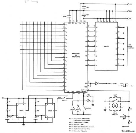
National MM5740 encoder serves as interface between keyboard and MM5204 4K PR0M capable of handling 90 four-mode keys. Encoder includes all Iogic needed for key validation, two-key or N-key rollover, bounce masking, mode selection, and strobe generation. Key code outputs can be defined by user. Bit-paired coding system of en coder has five common bits (B1-B4 and B9) and four variable bits (B5-B8) for each key. Each keyswitch is defined by one X drive line and one Y sense line of encoder,Combinationgives totalof 360 9-bit codes,-''Memory ApplicationsHandbook,'' National Semiconductor,SantaClara,CA,1978,p 5-⒌-5-8.
(View)
View full Circuit Diagram | Comments | Reading(982)
| Pages:198/471 At 20181182183184185186187188189190191192193194195196197198199200Under 20 |
Circuit Categories
power supply circuit
Amplifier Circuit
Basic Circuit
LED and Light Circuit
Sensor Circuit
Signal Processing
Electrical Equipment Circuit
Control Circuit
Remote Control Circuit
A/D-D/A Converter Circuit
Audio Circuit
Measuring and Test Circuit
Communication Circuit
Computer-Related Circuit
555 Circuit
Automotive Circuit
Repairing Circuit