
Index 184
COIN_TOSSER
Published:2009/7/13 3:23:00 Author:May
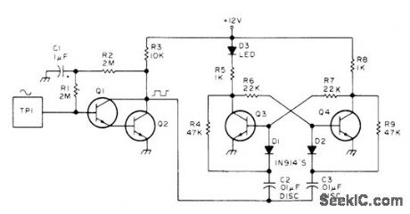
Finger on touch plate TR1 feeds stray 60-Hz sine wave (picked up by body capacitance) to high-impedance Darlington pair Q1-Q2 for squaring. Output drives flip-flop Q3-Q4. LED conducts only when Q3 is on. Removal of finger leaves LED eitheron or off with random probability. Players can try in turn to match, play odd-man-buys, or play odd-man-out. For faster results, circuit can be duplicated so each player has own touch plate. Practically any transistor types can be used, as circuit is not criti-caL-J. H. Everhart, The Coffee Flipper, 73Magazine, Nov. 1976, p 162-163. (View)
View full Circuit Diagram | Comments | Reading(1408)
TV_LINE_DECODER_I
Published:2009/7/13 3:21:00 Author:May
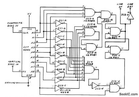
This circuit will produce outputs on TV lines 24 and 257. It was used for a decoder circuit. It uses a CMOS counter and gate logic. Only one pin is used for the output line indicator. (View)
View full Circuit Diagram | Comments | Reading(714)
ALPHANUMERIC_PAGER_DECODER
Published:2009/7/13 3:20:00 Author:May
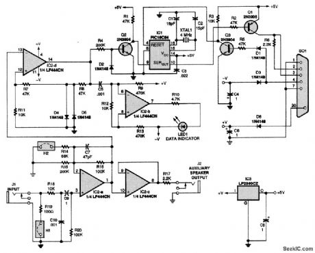
This pager decoder interfaces a scanner plugged into J1 with a personal computer's serial port via the DB25 connector. Software is necessary and can be obtained from the Internet at http://cylexinc.com/download.htm. (View)
View full Circuit Diagram | Comments | Reading(1011)
TICK_TACK_TOE_MEMORY
Published:2009/7/16 3:56:00 Author:Jessie
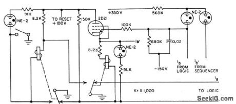
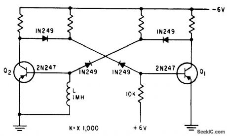
Nine memory cells are used, one for each position on game board. Circuit shown is for position No. 1. Operator moves are entered into board by pushbuttons on display panel, energizing self-latching relays of memory. Board moves are determined by a separate logic section that triggers thyratron of memory and energizes relay. Neon lamps indicate when each position is filled, and by whom.-C. E. Hendrix and R, B. Purcell, Neon Lamp Logic Gales Play Tick-Tack-Toe, Electronics, 31:25,p 68-69. (View)
View full Circuit Diagram | Comments | Reading(1010)
CORES_ACTUATE_RELAY
Published:2009/7/13 3:18:00 Author:May
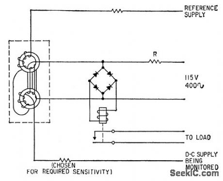


When d-c supply voltage equals reference voltage, no direct current flows through the control windings of saturable reactors, reactance of 400-cps winding is high, and voltage across rectifier bridge is high enough to pull in relay. When supply voltage increases or decreases, difference voltage causes core saturation that reduces reactance, allowing relay to drop out. Neon indicator lamp may be used in place of rectilfier bridge.-M. C. Herzig and D. C. Colbert, Voltage Monitor Needs Only Two Saturable Cores, Electronics, 36:23, p50-51. (View)
View full Circuit Diagram | Comments | Reading(759)
BASIC_IC_GATE
Published:2009/7/16 3:56:00 Author:Jessie

Circuit is basic element of current mode logic family. If reference voltage VBB is supplied to one side of gate, constant current that normally Bows through 1.24 K emitter resistor can be switched from one side of gate to other by switching input signals above and below reference voltage. Complementary output is provided from single gate.-S. T. Robertson, Integrated Circuit Line Driver, Motorola Application Note AN-187, Aug. 1965. (View)
View full Circuit Diagram | Comments | Reading(714)
QUAD_BLOCK
Published:2009/7/16 3:55:00 Author:Jessie

With appropriate interconnections of external terminals, can be used either as binary counter, monostable mvbr, Schmitt trigger, or selector. Although original design uses encapsulated construction, can readily be adapted for integrated circuit production techniques. Requires 10 ma for all applications, and gives output pulses with 0.1 microsec rise time and up to 0.4 microsec fall time.-F. K. Luteran, Four-Way Quad Circuit Building Block, EEE, 10:6, p 66-67. (View)
View full Circuit Diagram | Comments | Reading(861)
PARALLEL_PNP_BASIC_LOGlC
Published:2009/7/16 3:55:00 Author:Jessie
Serves as or gate for normally open switches and as and gate for normally closed switches. Provides phase inversion of input.-Texas Instruments Inc., Transistor Circuit Design, McGraw-Hill, N.Y., 1963, p 388. (View)
View full Circuit Diagram | Comments | Reading(674)
GROUNDED_LINE_CABLE_DRIVER
Published:2009/7/13 3:14:00 Author:May
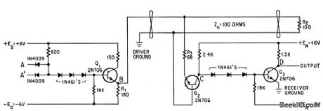
Twisted 100 ohm d-c coupled tranmission line solves ground-differential problem between driving and receiving subsystems up to 120 feet apart, while eliminating costly transformer coupling. Holding line excursion to 1.5V minimizes capacitive crosstalk. Up to four receivers can be used on one line.-R. C.Garavalia.Transimission lines Couple Multiple-Driver Receivers.Electronics.39:16,p121-122. (View)
View full Circuit Diagram | Comments | Reading(652)
TRANSFORMERLESS_DC_TO_DC_CONVERTER
Published:2009/7/13 3:14:00 Author:May
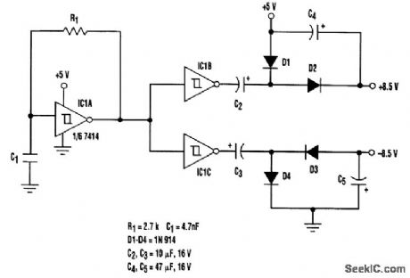
This configuration should prove handy in situations in which dual-polarity supplies are needed for a few devices on a board that has only one +5-V supply. The circuit doesn't need any dc-to-dc converter ICs, nor does it require any transformers or inductors. Three Schmitt-trigger inverters, such as the 7414, form the heart of the circuit (see the ftgure). One inverter is configured as a high-frequency astable multivil)rator employing a single resistor and a capacitor. For the RC values shown, the frequency of the astable output is around 100 kHz. The frequency of the oscillation is given by f=1/T, where T=R1C1 ln[1-VCC/VLT)/(1-VCC/VUT)] and R1 and C1 are the timing components of the astable multivibrator, VCC is the supply voltage, and VLT and VUT are the lower trip point and upper trip point of the Schmitt trigger. The astable multivibrator's output drives a pair of inverters that, in turn, drive a pair of diode-capacitor voltage-doubler circuits. The outputs of the diode-capacitor circuits are around 8.5 V with the polarities shown. Diodes D1 to D4 should be fast-switching types, like the 1N914 or 1N4148. As a result, the circuit can generate ±8.5 V from a single +5-V sup-ply making it useful in many applications. (View)
View full Circuit Diagram | Comments | Reading(1471)
PARALLEL_NPN_BASIC_LOGIC
Published:2009/7/16 3:54:00 Author:Jessie
Serves as or gate for normally open switches and as and gate for normally closed switches. Provides phase inversion of input.-Texas Instruments Inc., Transistor Circuit Design, McGraw-Hill, N.Y., 1963, p 388. (View)
View full Circuit Diagram | Comments | Reading(745)
ADC_CONTROLLING_DIGITAL_POTENTIOMETER
Published:2009/7/13 3:09:00 Author:May
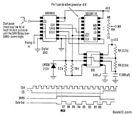
This design was created to control a DS1267 digital potentiometer with an analog signal. The DS1267 is a dual-pot chip, but this design will enable control of only one section. Here, the analog-to-digital converter (ADC) used is an ADC0833 8-bit serial I/O converter with a four-channel multi-plexer. The analog input to channel 3 of the ADC is employed. The timing diagram illustrates the operation of the circuit. A negative start pulse on the chip select of the ADC starts the sequence (the pulse must stay low for at least 14 clock pulses or until the ADC's SAR Status line comes high). The next five clock pulses perform various housekeeping in the ADC, The Data 0ut line comes out of tristate on the negative edge of the fifth pulse, and the SAR Status line comes high to signal a conversion in progress. The first bit on the Data Out line is a leading zero for one clock period. Data is clocked into the DS1267 on the positive edge of the clock pulse. The input format for the DS1267 requires that the first bit determine the stack select (used in the DS1267 when the two pots are com-bined) and the following 8 bits provide data. Following transmission of these 9 bits, the SAR Status line goes high, disabling further input to the DSl267 (the ADC0833's output format continues trans-mission of 8 more bits of the conversion in reverse order, but the DS1267 ignores these). Input range for the ADC is 0 to 5 V. Pin 1 of the DS1267 is shown tied to ground (for pot connections referenced to ground; however, -SVcan be used to provide a range of 15 to -5 V on the pot). (View)
View full Circuit Diagram | Comments | Reading(3470)
VOICE_OPERATED_MACHINE_CONTROL
Published:2009/7/13 3:08:00 Author:May
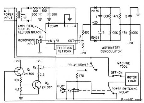
Circuit rejects ambient noise or normal speech but responds to sharply spoken commands during emergency, to open motor circuit of machine tool. Asymmetry demodulator rejects symmetrical noise while accepting speech vowels having strong asymmetry.-W.C.Dersch.Speech Operates Safety Switch.Electronics.36:25,p78-82 (View)
View full Circuit Diagram | Comments | Reading(677)
CURRENT_LIMITING_A_SERIES_REGULATOR
Published:2009/7/13 3:07:00 Author:May
If the current limitation of the series-pass transistor is exceeded, transistor Q1 could be damaged or destroyed. This can be prevented with the addition of a current-limiting transistor, as shown in the figure. When the current through Q1 becomes high enough, the voltage drop across R2 becomes high enough to forward-bias transistor Q2. When Q2 starts to conduct, its internal resistance decreases. When this occurs, the forward bias of Q1 is fixed, and its output is a constant current. The current-limiting transistor and resistor in the figure protect the pass transistor and rectifier diodes if the load terminals are accidentally short-circuited. However, the addition of transistor Q2 increases the already high power dissipation in pass transistor Q1 when the load demand is high. (View)
View full Circuit Diagram | Comments | Reading(710)
TOUCH_PLATE_RELAY
Published:2009/7/13 3:06:00 Author:May
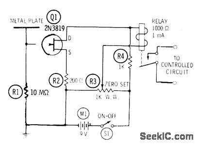
When 2-inch diameter disk of sheet metal or foil is firmly touched with finger, stray noise picked up by body and coupled into 10-megohm gate circuit of FET is sufficient to boost drain current to about 1.7 mA and close relay. Delayed dropout can be obtained by placing capacitor in parallel with relay coil; delay is about 0.8 s per 1000 μF of parallel capacitance.-R. P. Tumer, FET Circuits, Howard W. Sams, lndianapolis, IN, 1977, 2nd Ed., p 104-105. (View)
View full Circuit Diagram | Comments | Reading(1145)
90_VRMS_AT_500_W
Published:2009/7/13 3:05:00 Author:May

Open-loop RMS voltage regulator acts with full-wave bridge to provide good AC voltage regulation for AC load over line voltage range of 110-130 VAC. As input voltage increases, voltage across R10 increases andserves to increase firing point of PUT Q3. This delays firing of SCR Q5 to hold output voltage fairly constant as input voltage increases. Delay network of Q1 prevents circuit from latching up at beginning of each charging cycle for C1.-R.J. Haver and B.C. Shiner,″Theory,Characteristics and Applications of the Programmable Unijunction Transistor, Motorola,Phoenix,AZ,1974,AN-527,p 11. (View)
View full Circuit Diagram | Comments | Reading(1789)
DATA_ENTRY
Published:2009/7/13 3:04:00 Author:May
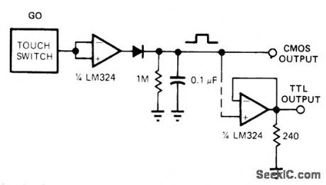
Touch of operator's finger on input button produces CMOS output. Addition of one opamp section gives TTL output. Touch button can be 0.5-inch-square copper-clad pattern on printed-circuit board or machine-screw head having comparable area. For proper switching, circuit must connect to line-operated DC power supply.-R. D. Wood, Replace Bulky Mechanical Switches with Touch Controls, EDN Magazine, April 20, 1978, p 132-133. (View)
View full Circuit Diagram | Comments | Reading(909)
UNDERCURRENT_OVERCURRENT_PROTECTION
Published:2009/7/13 3:04:00 Author:May
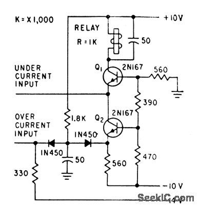
Guards against improper operation of control amplifier in nucelor reator scram system.If rod currents vary beyond predetermined limits circuit initiates reactor scram.Either transistor may open relay coil circuit.-E.J.Wade and D.S.Davidson.How Transistor Circuits Protect Atomic Reactors,Electronics.31:29.p73-75. (View)
View full Circuit Diagram | Comments | Reading(1065)
CHOKE_CONTROLLED_ONE_SHOT
Published:2009/7/16 10:17:00 Author:Jessie
Provids output pulses longer in duration than input trigger. Can be triggered by either negative or positive pulse. –W. M. Carey,Using Inductive Control in Computer Circuits, Electronics, 32:38, p 31-33. (View)
View full Circuit Diagram | Comments | Reading(534)
12_V_REGULATOR_FOR_GTL_TERMINATION
Published:2009/7/13 3:02:00 Author:May
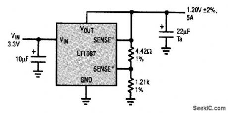
A recent development in high-speed digital design has resulted in a new family of logic chips called gunning transition Logic (GTL). These chips use high-speed logic and require active termination for best interconnection performance. The termination voltage required is 1.2 V, and the input voltage can be as low as 3.3 V from a logic supply. The LT1087 5-A low-dropout regulator shown here addresses these requirements by providing a regulated 1.2-V ±2 percent output voltage from a minimum 2.7-V input. Note that the LT1087 has a 1.25-V reference, but provides Kelvin sensing inputs for the feedback amplifier. The 4.42-Ω resistor is inserted as a simple way to adjust the internal reference downward without sacrificing regulation. This GTL termination circuit supplies 5 A maximum load current and can handle 3.3-, 5-V, or higher supplies, although 3.3 V is recommended for minimum device dissipation. (View)
View full Circuit Diagram | Comments | Reading(893)
| Pages:184/471 At 20181182183184185186187188189190191192193194195196197198199200Under 20 |
Circuit Categories
power supply circuit
Amplifier Circuit
Basic Circuit
LED and Light Circuit
Sensor Circuit
Signal Processing
Electrical Equipment Circuit
Control Circuit
Remote Control Circuit
A/D-D/A Converter Circuit
Audio Circuit
Measuring and Test Circuit
Communication Circuit
Computer-Related Circuit
555 Circuit
Automotive Circuit
Repairing Circuit