
Index 183
NE602_PRODUCT_DETECTOR_CIRCUIT
Published:2009/7/13 3:43:00 Author:May
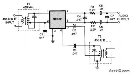
This circuit uses an NE602 as a product detector. The component values depend on operating frequency and are typical for 455-kHz operation. Note that a passive RC filter is showtt in the audio output circuit. T2 acts as an oscillator coil for the 455-kHz local oscillator (or, in this case, beat frequency oscillator). (View)
View full Circuit Diagram | Comments | Reading(4102)
ABSOLUTE_DIFFERENCE_INTEGRATOR
Published:2009/7/16 4:02:00 Author:Jessie
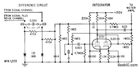
Uses two-pole chopper with capacitor connected between the two reeds. During half of chopper cycle, capacitor is charged to voltage difference between outputs of two signal-processing channels. During other half-cycle, charge is transferred to integrator circuit and positive side of capacitor is clomped to ground by one of the two diodes. Integrator is chopper-stabilized d-c amplifier with capacitive feedback, having gain of 200 and integration time constant of 1.5 hours.-H. Schwarzlander, Intelligibility Evaluation of Voice Communications, Electronics, 32:22, p 88-91. (View)
View full Circuit Diagram | Comments | Reading(645)
ONE_IC_TONE_DECODER
Published:2009/7/13 3:42:00 Author:May
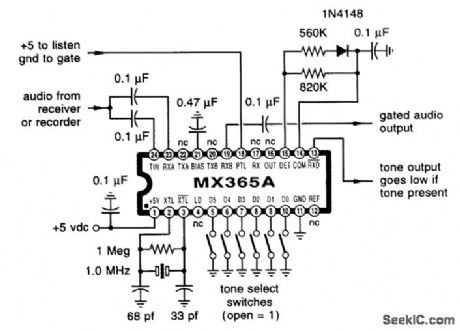
This circuit can be used in a receiver or a repeater to require that a tone be present on a received signal so as to unsquelch the receiver. (View)
View full Circuit Diagram | Comments | Reading(584)
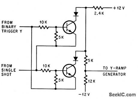
INTEGRATOR_AND_BINARY_TRIGGER_FOR_SHMOO_PLOTTER
Published:2009/7/16 4:02:00 Author:Jessie
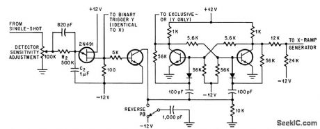
Integrator stage with R2-C2 measures duty cycle of single-shot mvbr used in showing computer memory perform once under marginal drive currents. Binary triggers control direction of ramp generators und increase or decrease memory drive current. Npn transistors are 2N706 and diodes are 1N921.-J. E. Gersbach, The Great Shmoo Plot: Testing Memories Automatically, Electronics, 39:15, p 127-134. (View)
View full Circuit Diagram | Comments | Reading(709)
BCD_DECODER_DRIVER_CIRCUIT
Published:2009/7/13 3:41:00 Author:May
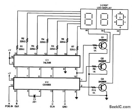
The BCD decoder-driver circuit will interface with any standard BCD output to produce a digital display. (View)
View full Circuit Diagram | Comments | Reading(1320)
RTTY_TONE_DECODER
Published:2009/7/13 3:40:00 Author:May
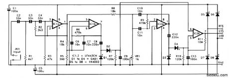


The full circuit diagram for the RTTY tone decoder is shown. The input filter is based on IC1a, and it is a third-order (18 dB per octave) high-pass type with a cutoff frequency at approximately 750 Hz. IC1b is used in the higher-frequency bandpass filter. Capacitor C8 couples the output of this filter to a conventional half-wave rectifier and smoothing network based on diodes D1 and D2. The time constant of R7 and C9 is long enough to give a well-smoothed output signal, but short enough to permit the unit to respond rapidly as the input signal alternates between one tone and the other. The second bandpass filter is based on IC2a and is essentially the same as the first, but it has a preset resistor (VR1) as one section of the input attenuator. This enables the center frequency of the filter to be adjusted, but (in operation) it is set 170 Hz lower than the center frequency of the other filter. If preferred, preset potentiometer VR1 can be set to give a center frequency 170 Hz higher than the other filter. It can also be set for shifts of other than 170 Hz.The output of IC2a (pin 1) feeds into a rectifier and smoothing circuit that is identical to the one used at the output of the other filter.The outputs of both the smoothing circuits drive the inputs of IC2b, which acts as the voltage comparator. A small amount of dc positive feedback is provided by resistor R11, and this helps to avoid problems with jitter at the output when only background noise is present at the input. Power is obtained from two of the otherwise unused handshake outputs of the PC's serial port. Diodes D5 to D8 form a bridge rectifier that ensures that the circuit is always provided with a supply of the correct polarity. Only a milliampere or two can be drawn from the handshake outputs. Accordingly, IC1 and IC2 must be low-supply-current operational amplifiers. (View)
View full Circuit Diagram | Comments | Reading(1774)
BISTABLE_AND_CIRCUIT_WITH_RESET
Published:2009/7/16 4:01:00 Author:Jessie
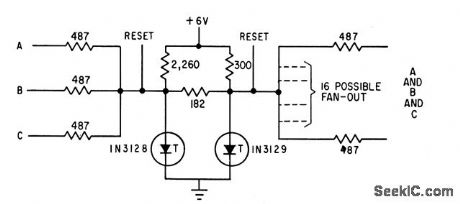
Uses resistance-coupled inputs to tunnel diodes. Gate is open when 1N3l29 is on its negative-resistance slope, so reset pulse must be applied to close if.-F. Leary, Computers Today, Electronics, 34:17, p 64-94. (View)
View full Circuit Diagram | Comments | Reading(569)
R_C_SERVO_SWEEP_DRIVER_CIRCUIT
Published:2009/7/13 3:37:00 Author:May
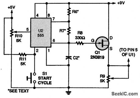
The circuit shown produces a ramp that can be used to modulate the threshold of another 555 timer, which is configured to generate the pulse signal to drive the R/C servo. In this way, the servo can be slowly moved through a desired angle. Note that for long time constants, R6 and R7 will be large. Therefore, C2 should be a low-leakage capacitor, or a CMOS timer (7555) can be used to permit larger resistances and smaller capacitors to be used. (View)
View full Circuit Diagram | Comments | Reading(754)
DTMF_RECEIVER_DECODER
Published:2009/7/13 3:36:00 Author:May
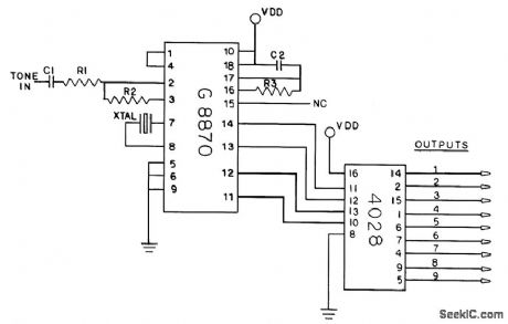
This decoder uses a G8870 DTMF receiver decoder chip to decode DTMF signals and drive individual outputs via a 4028 binary-decimal decoder. Xtal is a 3.579-MHz TV burst crystal. C1=C2=0.1μF, R1=R2=100 kΩ and R3=300 kΩ. D1 through D4 are small red LEDs. (View)
View full Circuit Diagram | Comments | Reading(3631)
DTMF_DECODER_II
Published:2009/7/13 3:34:00 Author:May

This decoder uses a 68870 DTMF receiver decoder chip to decode DTMF signals and display them in binary via LEDs. Xtal is a 3.579-MHz TV burst crystal. C1=C2=0.1μF, R1=R2=100 kΩ, and R3=300 kΩ. D1 through D4 are small red LEDs. (View)
View full Circuit Diagram | Comments | Reading(3319)
FLIP_FLOP_FOR_SHIFT_REGISTER
Published:2009/7/16 4:00:00 Author:Jessie
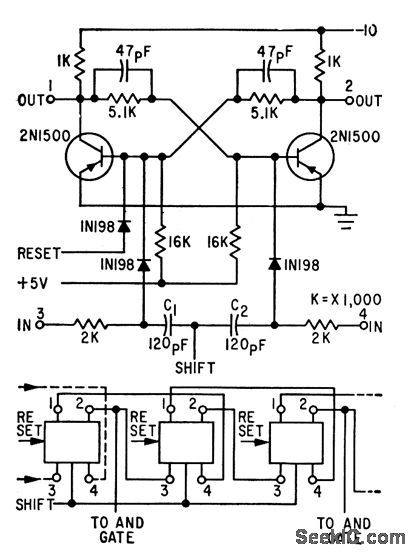
Used to pro duce complex pulse sequences up to 4 billion bits in length, at frequencies up to 1.5 Mc-Each flip-flop provides 10 ma when turned on and draws 0.6 ma when off.-B. K. Ericksen and J. D Schmidt, Random Pulse Generator Tests Circuits, Encodes Messages, Electronics, 34:25, p 56-59. (View)
View full Circuit Diagram | Comments | Reading(799)
MICROWAVE_REFLECTION_ANTENNA
Published:2009/7/13 3:33:00 Author:May
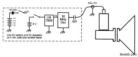
Originally used for 10-GHz microwave transmitter testing, this antenna modulates a received signal with 30 MHz and reflects it, producing a signal component 30 MHz offset from the incident signal for reception and dish-aiming tests. (View)
View full Circuit Diagram | Comments | Reading(3355)
BALUN_BOX
Published:2009/7/13 3:32:00 Author:May
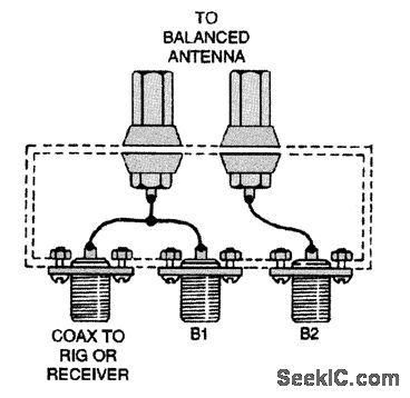
Here's the connection box for making a 4:1 coaxial balun. It is intended for mounting on antenna center isolator. (View)
View full Circuit Diagram | Comments | Reading(883)
10_GHz_WAVEGUIDE_TEST_ANTENNA_SETUP
Published:2009/7/13 3:31:00 Author:May
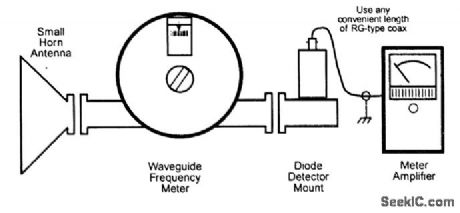
This waveguide test antenna, wavemeter, and meter amplifier setup uses a small horn antenna and a variable commercial waveguide frequency meter to determine RF frequency. RF is sampled with a detector and displayed on an amplified meter for sensitive meter indications. (View)
View full Circuit Diagram | Comments | Reading(957)
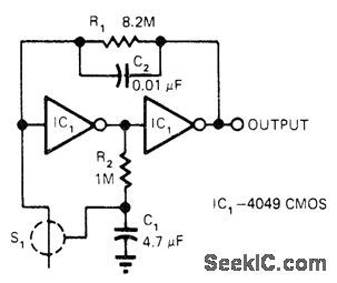
HIGH_GAIN_AUDIOPREAMP
Published:2009/7/16 3:59:00 Author:Jessie
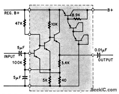
Has strong negative feedback and built-in power supply series regulator.-D. D. Robinson, Linear Microcircuits Scarce? Now You Can Breadboard Your Own, Electronics, 37:27, p 58-64. (View)
View full Circuit Diagram | Comments | Reading(640)
COMPLEMENTARY_TRANSISTOR_LOGIC
Published:2009/7/16 3:59:00 Author:Jessie
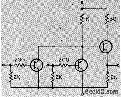
Uses both pnp and npn transistors, with pnp emitters tied together and returned through 1K resistor to positive voltage supply. Propagation delay is 3 to 5 nsec for fanouts of 1 to 10.-D. Christiansen, Logic Schemes Reviewed, EEE, 13:11, p 64-79, (View)
View full Circuit Diagram | Comments | Reading(755)
DTMF_DECODER_I
Published:2009/7/13 3:27:00 Author:May
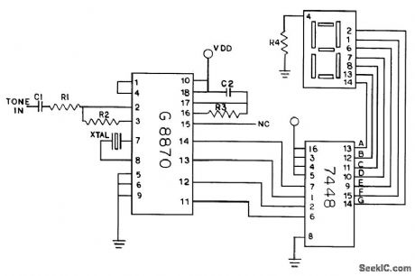
This decoder uses a G8870 DTMF receiver decoder chip to decode DTMF signals and display them via an LED display driven by a 7448 decoder driver chip. Xtal is a 3.579-MHz TV burst crystal.C1=C2-0.1μF, R1=R2=100 kΩ.and R3=300 kΩ. D1 through D4 are small red LEDs. (View)
View full Circuit Diagram | Comments | Reading(6858)
EXCLUSIVE_OR_CIRCUIT
Published:2009/7/16 3:58:00 Author:Jessie
Used in tester that shows computer memory performance under marginal drive currents by plotting shmoo curves. Memory error triggers single-shot and changes direction of Y generator from positive to negative along top of shmoo curve, and from negative to positive along bottom. Transistors are 2N706 and diodes ore 1N921.-J. E. Gersbach, The Great Shmoo Plot: Testing Memories Automatically, Electronics, 39:15, p 127-134. (View)
View full Circuit Diagram | Comments | Reading(931)
TOUCH_SWITCH_USES_TIMER
Published:2009/7/13 3:24:00 Author:May
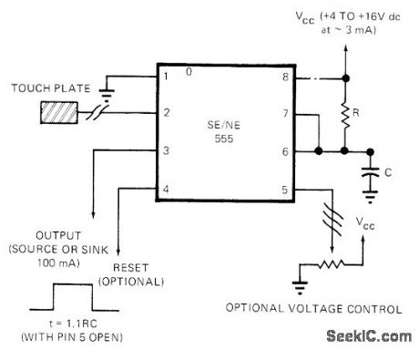
Free-running or mono capabilities of Signetics 555 timer can be controlled through choice of trigger and reset inputs, Characteristics of output pulses can be adiusted over timing periods ranging from microseconds to hours. With 5-V supply, output is TTL-compatible and current drain of only 3 mA perrnhs battery operation. Circuit is easily triggered by voltage differential between floating (ungrounded) human body and timer itself.Touch plate can be any conducting material, with virtually no size limitation. Once triggered by momentary touch, device cannot be retriggered until it has timed out. Duration of output pulse depends on RC time constant and on control voltage. Applications include switchless keyboards, burglar alarms, and bouncefree switches.-J. C. Heater, Monolithic Timer Makes Convenient Touch Switch, EDN Magazine, Dec. 1, 1972, p 55. (View)
View full Circuit Diagram | Comments | Reading(843)
TV_LINE_DECODER_II
Published:2009/7/13 3:24:00 Author:May
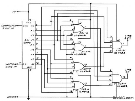
This circuit will produce outputs on TV channels 24 and 25.It was used in a decoder circuit. Ituses a CMOS counter and gate logic. (View)
View full Circuit Diagram | Comments | Reading(1382)
| Pages:183/471 At 20181182183184185186187188189190191192193194195196197198199200Under 20 |
Circuit Categories
power supply circuit
Amplifier Circuit
Basic Circuit
LED and Light Circuit
Sensor Circuit
Signal Processing
Electrical Equipment Circuit
Control Circuit
Remote Control Circuit
A/D-D/A Converter Circuit
Audio Circuit
Measuring and Test Circuit
Communication Circuit
Computer-Related Circuit
555 Circuit
Automotive Circuit
Repairing Circuit