
Index 195
10_min_DELAY
Published:2009/7/12 20:52:00 Author:May
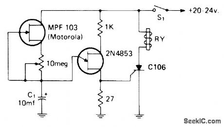
MPF103 JFET makes charging current of C1 constant regardless of degree of charge, to give longer charging time and longer timedelay. After delay determined by setting of 10-megohm pot, UJT conducts and discharges Q, through 27-ohm resistor, triggering SCR and energizing relay. Open S1 to reset circuit.-I. Math, Math's Notes, CQ, April 1974, p 64-65 and 91-92. (View)
View full Circuit Diagram | Comments | Reading(674)
APPLIANCE_TIMER
Published:2009/7/12 20:50:00 Author:May
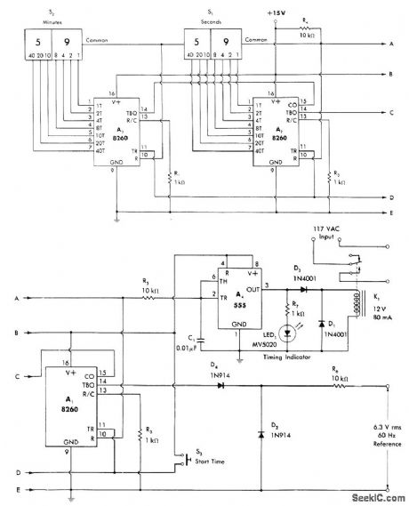
Controls intervals up to 1 h in 1-s increments as programmed by thumb wheel switches S1 and S2. Circuit is basically two-stage programmed counter driven by 1-s clock derived from 60-Hz power line. A1 is connected as divide-by-60 counter triggered by 60-Hz signal developed across D2. 1-Hz output from A1 triggers A2 which in tum triggers A3, all programmable timers. When S3 is closed, R4 bus goes low to start timing cycle. Relay driver A4 holds relay K1 closed for application of AC power to device being controlled and energizing of LED to indicate active timing cycle. Applications include uses as kitchen and darkroom timers,-W. G. Jung, IC Timer Cookbook, Howard W. Sams, Indianapolis, IN, 1977, p 214-218. (View)
View full Circuit Diagram | Comments | Reading(1795)
INFRARED_CODE_PRACTICE_RECEIVER
Published:2009/7/12 20:47:00 Author:May
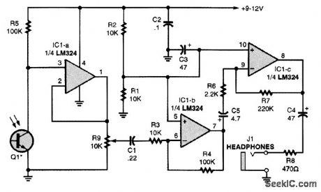
An IR phototransistor, Q1, is directly-coupled to the input of op amp IC1-a. The output of IC1-a is fed through the gain-control potentiometer R9 to the input of op amp IC1-b, which has a voltage gain of 10. Section IC1-b's output drives IC1-c, which has a voltage gain of 100. The output of IC1-c supplies audio to the heddphones via J1. The IR phototransistor can be mounted in reflectors to increase the CPO's operating range. (View)
View full Circuit Diagram | Comments | Reading(1576)
REPEAT_CYCLE
Published:2009/7/12 20:47:00 Author:May
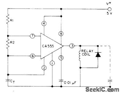
RCA CA555 is connected for astable operation in which total period is sum of individual perids t1 and t2, where t1 = 0.693(R1 + R2)CT and t2 = 0.693R2CT. With 5-V supply, output voltage has rectangular pulses with interval t1 separated by interval t2. With optional capacitor connected, voltage across capacitor is sawtooth that rises for interval t1 and decays for interval t2.- Linear Integrated Circuits and MOS/ FET's, RCA Solid State Division, Somerville, NJ, 1977, p 56. (View)
View full Circuit Diagram | Comments | Reading(669)
SOLID_STATE_TURNOFF_DELAY
Published:2009/7/12 20:45:00 Author:May
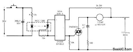
Designed for applications where machine must remain energized for certain period of time after some other operation has stopped, as when pump motor must run long enough to dear pipes in chemical plant. When switch is closed, LED of optoisolator is forward-biased and turned on, making photoGCR conduct and provide gate current via MDA920-4 diode bridge fortriac. Values shown keep solid-state relay circuit on for about 5 s after pushbutton is released. Resistor and capacitor values can be changed to obtain different delay.-T. Mazur, Solid-State Relays Offer New Solutions to Many Old Problems, EDN Magazine, Nov. 20, 1973, p 26-32. (View)
View full Circuit Diagram | Comments | Reading(593)
ORYSTAL_CONTROLLED_CODE_PRACTICE_TRANSMITTER
Published:2009/7/12 20:39:00 Author:May
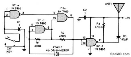
When the CW key is closed, IC1-a's output goes high, allowing IC1-b and IC1-c to oscillate. The crystal supplies the feedback path setting the oscillator's operating frequency. The circuit will operate on the 40- and 80-m bands. Section IC1-d isolates the oscillator from the short antenna, ANT1. A clip lead should do here to get the signal out and about for operation. Tune your ham-band receiver to the crystal's frequency and key down. If the receiver doesn't have a CW mode, turn on the BFO and tune for the desired CW tone. (View)
View full Circuit Diagram | Comments | Reading(679)
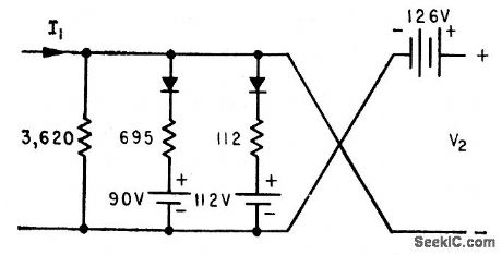
DRIVE_FOR_THIN_FILM_MEMORY
Published:2009/7/12 20:38:00 Author:May
Has single pulse output when input blocking oscillator is triggered by single positive-going pulse, for driving film alternately from one remanence to another in astatic loop.-S. Feinstein and H. J. Weber, Electrical Readout from Thin Ferromagnetic Films, Electronics, 33:31, p100-102. (View)
View full Circuit Diagram | Comments | Reading(580)
HALF_ADDER
Published:2009/7/12 20:36:00 Author:May

Uses four-point matrix of pnp junction switching transistors, whh bases and emitters cross-connected. Input A can be switched to base of Q1 or Q2. Input B can be switched between two alternate sets of emitters. For any input switch position, only one transistor is conducting.-F. B. Maynard, Half-Adders Drive Simultaneous Computer, Electtonics,31:29,p80-82. (View)
View full Circuit Diagram | Comments | Reading(1019)
LOW_POWER_WIDE_SUPPLY_RANGE_CLOCK
Published:2009/7/12 20:34:00 Author:May
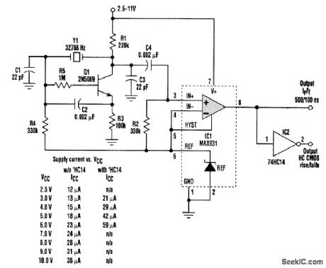
This 32-kHz, low-power clock oscillator offers numerous advantages over conventional oscillator circuits based on a CMOS inverter.Many times, 32-kHz oscillators are used to generate a system clock or an auxiliary sleep clock in low-power instruments and microcontrollers. The typical implementation uses a CMOS inverter (74HC04 or CD4049UB type). Inverter circuits present problems, though. Supply currents fluctuate widely over a 3- to 6-V supply range, and currents below 250 μA are difficult to attain. Operation can be unreliable for wide variations in supply voltage. A very low power crystal oscillator solves these problems. Drawing only 13μA from a 3-V supply, it consists of a single-transistor amplifier/oscillator (Q1) and a low-power comparator/reference device (IC1). Q1's base is biased at 1.25V via R5, R4, and the reference in IC1. VBE is about 0.7 V, placing the emitter at approximately 0.5 V. This constant voltage across R3 sets the transistor's quiescent current at 5μA, which fixes the collector voltage at about 1 V below VCC. The amplifier's nominal gain (R1/R2) is approximately 2 V/V The crystal and load capacitors (C1 attd C3) form a feedback path around Q1, whose 180°of phase shift causes the oscillation. C4 couple this singal to the comparator input;the input's quiescent voltage (1.25V) is set by the reference via R2.The comparator's input swing is thus centered around the reference voltage. Operating at 3V and 32 KHz,IC1 draws about 7μA. (View)
View full Circuit Diagram | Comments | Reading(1634)
CLOCK_GATE
Published:2009/7/12 20:32:00 Author:May
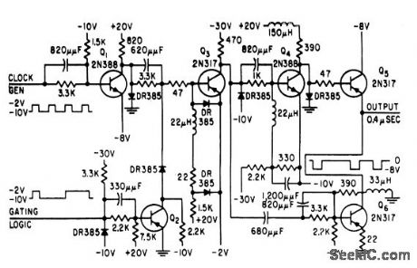


Provides effective gating with negligible insertion loss. Used as part of clock driver for developing and testing large digital computers.-S.Schoen,Transisitors Provide Computer Clock Signals.Electronics.32:9,p70-72 (View)
View full Circuit Diagram | Comments | Reading(610)
RECIPROCAL_CIRCUIT
Published:2009/7/12 20:18:00 Author:May
Output is inversely proportional to input. Article gives design procedure based on use of diodes, resistors, and d-c voltage supplies.-A. Gill, Procedure for Designing Reciprocal Computer Circuits, Electronics, 33:21, p92-93. (View)
View full Circuit Diagram | Comments | Reading(888)
THIN_FILM_MEMORY_READOUT
Published:2009/7/12 20:14:00 Author:May


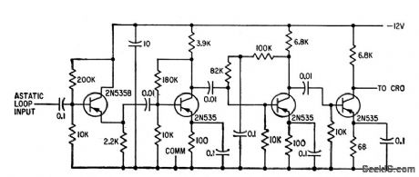
High-gain am plifier has gain of 65 db and produces saturated output for cro.-S. Feinstein and H. J.Weber,Electrical Readout from Thin Ferromagnetic Films,Electronics,33:31,p100-102. (View)
View full Circuit Diagram | Comments | Reading(593)
VOLTAGE_TO-FREQUENCY_CONVERTER_WITH_OPTOCOUPLER
Published:2009/7/11 5:31:00 Author:May

In this circuit, a Raytheon RC4151 or National LM131 is used in conjunction with an optocoupler for applications where input-to-output isolation is desirable. Circuit values are shown in the figure for various applications. (View)
View full Circuit Diagram | Comments | Reading(2032)
SIMPLE_LOW_FREQUENCY_V_F_CONVERTER
Published:2009/7/11 5:28:00 Author:May
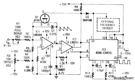
In this circuit, C1 is charged to a fixed reference level, then discharged. Integrator IC1 circuit charges C1 until IC1 has -6.2-V output, when comparator IC2 outputs a low. FET Q1, triggers one-section monostable multivibrator IC3, pulls pin 3 1ow for 470 μs, ensuring that Q1 completely discharges C1. The other section of IC3 produces a longer pulse of about 47 ms.Full scale of this circuit is 10 Hz. For lower output pulse rates, a counter circuit can be inserted between the sections of IC3. Notice that because C1 does not integrate while Q1 is biased on, this circuit has an error in the output period, which must be as short as possible. Therefore, the circuit's use is limited to low frequencies. (View)
View full Circuit Diagram | Comments | Reading(1499)
AF_SIGNAL_TRACER
Published:2009/7/11 5:26:00 Author:May
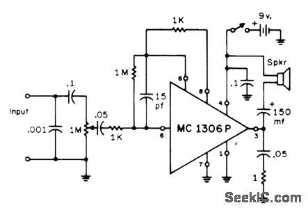
Motorola MC1306P complementary power amplifier delivers 1/2 W into loudspeaker for 3-mVRMS input to preamp, for troubleshooting all types of audio equipment. Zero-signal current drain is only 4 mA with 9-V supply. For RF tracing of modulated AM or SSB signal, use demodulator probe at input.-W. M, Scherer, High-Gain Signal Tracer, CQ, July 1972, p 12 and 14. (View)
View full Circuit Diagram | Comments | Reading(1209)
VOLTAGE-TO_FREQUENCY_CONVERTER_II
Published:2009/7/11 5:24:00 Author:May
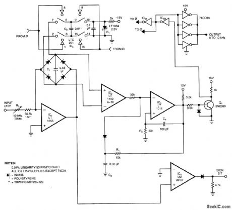
This voltage-to-frequency converter (VFC) accepts the bipolar-ac inputs. For -10- to + 10-V inputs, the converter produces a proportional 0- to 10-kHz output. Linearity is 0.04%, and temperature coefft-cient (TC) measures about 50 ppm/ °C.To understand the circuit, assume that its input sees a bipolar square wave. During the input's positive phase, IC1's output swings negative and drives current through C1 via the full-wave diode bridge. IC1's current causes C1's voltage to ramp up linearity. Instrumentation amplifier IC2 operates at a gain of 10 and measures the differential voltage across C1.IC2's output biases comparator IC3's negative input. When IC2's output crosses zero, IC3 fires ac positive feedback to IC3's positive input and hangs up IC3's output for about 20 μs. The Q1 level shifter drives ground-referred inverters IC5A and IC5B to deliver biphase drive to LT1004 switch IC6.IC6, configured as a charge pump, places C2 across C1 each time the inverters switch, which resets C1 to a lower voltage. The LT1004 reference (D1), along with C2's value, determines how much charge the charge pump removes from C1 each time the charge pump cycles. Thus, each time IC2's output tries to cross zero, the charge pump switches C2 across C1, which resets C1 to a small negative voltage and forces IC1 to begin recharging C1. The frequency of this oscillatory behavior is directly proportional to the input-derived current into IC1. During the time that C1 is ramping toward zero, IC6, places C2 across the reference diode (D1), and prepares C2 for the next discharge cycle. The action is the same for negative-input excursions, except that IC1's output phasing is reversed. IC2, looking differentially across IC1's diode bridge, sees the same signal as it does for positive inputs; therefore, the circuit's action is identical. IC4, detecting IC1's output polarity, provides a signal bid output. (View)
View full Circuit Diagram | Comments | Reading(1475)
VIDEO_SELECTOR
Published:2009/7/11 5:22:00 Author:May
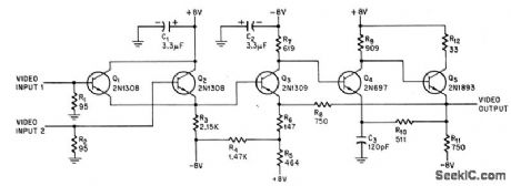
Selects largest of several positive-going video signals as positive-going output to 95-ohm load. Circuit gain is about 3 db.-A. E. Popodi, Reliable Repertoire of Display Circuits Electronics.38:2,p60-66 (View)
View full Circuit Diagram | Comments | Reading(1113)
28_MHz_TO_55_MHz
Published:2009/7/11 5:18:00 Author:May
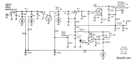
Contains bandpass filter, grounded-grid RF stage Q20, mixer Q21, and oscillator Q22, with all tuning accomplished by variable-capacitance diodes. Oscillator covers 22.5 to 24.5 MHz. Used in all-band double-con-version superheterodyne receiver for AM, nar-row-band FM, CW, and SSB operation. Supply is 13.6 V regulated. Article gives all circuits of receiver. -D.M Eisenberg, Build This All-Band VHF Receiver, 73 Magazine, Jan 1975, p 105-112 (View)
View full Circuit Diagram | Comments | Reading(597)
VOLTAGE_TO_FREQUENCY_CONVERTER_I
Published:2009/7/11 5:14:00 Author:May
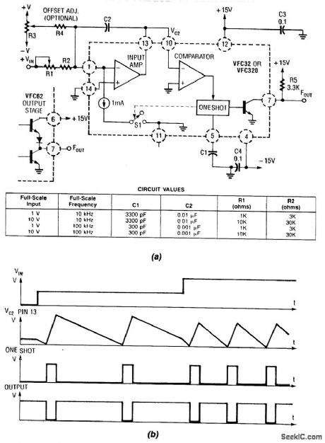
Using a Burr-Brown VFC 32 IC, this voltage-to-frequency convener uses few components. The circuit values are shown in the figure.This charge-balanced V/F converter uses a VFC32 or a VFC320 IC. The positive charge from the 1-mA balances the negative charge from the input. V/F converter waveforms are shown in Fig. 100-1(b). (View)
View full Circuit Diagram | Comments | Reading(769)
LOW_CURRENT_VOLTAGE_TRIPLER
Published:2009/7/11 5:08:00 Author:May
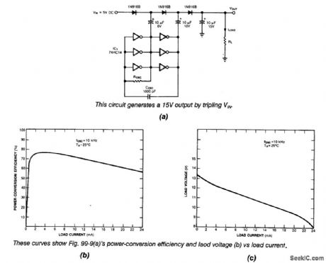
Using a 74HC14 operating at 350 kHz,this voltage tripler delivers approximately 12 V from a 5-V Supply. (View)
View full Circuit Diagram | Comments | Reading(563)
| Pages:195/471 At 20181182183184185186187188189190191192193194195196197198199200Under 20 |
Circuit Categories
power supply circuit
Amplifier Circuit
Basic Circuit
LED and Light Circuit
Sensor Circuit
Signal Processing
Electrical Equipment Circuit
Control Circuit
Remote Control Circuit
A/D-D/A Converter Circuit
Audio Circuit
Measuring and Test Circuit
Communication Circuit
Computer-Related Circuit
555 Circuit
Automotive Circuit
Repairing Circuit