
Index 191
STOPWATCH
Published:2009/7/12 22:45:00 Author:May
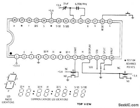
Intersil 7045 IC provides capability for driving digital display of time in hundredths of a second up through hours in four different operating modes selected by lower switches: sequential, standard, split, or rally. Grounding pin 9 momentarily with start switch initiates timing action. Repeated pressings of swhch activate operatirlg modes as selected. Grounding reset pin 16 clears stopwatch. IC can be connected directly to LED display, without drivers or resistors.-D. Lancaster, CMOS Cookbook, Howard W. Sams, Indianapolis, IN, 1977, p 159. (View)
View full Circuit Diagram | Comments | Reading(2467)
1000_V_FOR_CRT
Published:2009/7/12 22:43:00 Author:May
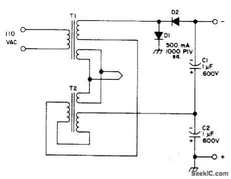
Unique connection of two TV boostertransformers having 125-V secondaries gives high-voltage supply for small monitor scope. T1 is connected conventionally, with its 6.3 V winding going to heater of CRT, 6.3-V winding of T2, also connected to CRT, serves as primary for second transformer. Remaining windings of T2 and high-voltage secondary of T1 are connected in series aiding to give about 367 VAC fordoubling by D1-D2 and C1-C2. Since CRT drain is low, filter charges to very nearly peak voltage of 1027 VDC.-W. P. Tumer,Cheap Power Supply for a CRT, 73 Magazine, March 1974, p 53. (View)
View full Circuit Diagram | Comments | Reading(881)
MICROSECONDS_TO_HOURS
Published:2009/7/12 22:42:00 Author:May
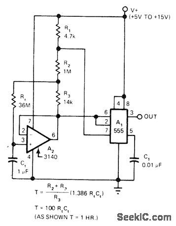
Timing range of 555 is increased 100 times by using 3140 FETinput opa mp in circuit that eff ectively multiplies values of timing components and buffers timing network, Pin 7 of 555 switches applied voltage of timing network between V+ and ground. Ratio selected for R2-R3 can be varied over wide range to change multiplying ratio, provided square-wave voitage across R3 is at least 50 mV. Output is essentially pure square wave. Supply voltage is notcritical.-W. G. Jung, Take a Fresh Look at New IC Timer Applications, EDN Magazine, March 20, 1977, p 127-135. (View)
View full Circuit Diagram | Comments | Reading(628)
SAFER_SECURITY_STSTEM
Published:2009/7/12 22:41:00 Author:May
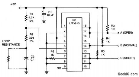
Many security systems use a closed loop of wires and switches, arranged so that whenever a door or window is opened, the loop will be broken and the alarm will sound. An obvious problem is that someone can tamper with the system, short out the loop, and later on come back and burglarize the premises without sounding the alarm. Hiding a known resistance in the loop is a very good idea. That way, the alarm can distinguish a short circuit from a correctly functioning closed loop. The figure shows a circuit that does the job. It is a somewhat unusual application for a National Semiconductor LM3915lC, normally used to drive LED bar-graph displays. That chip happens to contain the right combination of comparators and logic circuits to do what you need. Step 1 is to translate the loop resistance into a voltage. That is done by putting a voltage divider with resistors R1 and R2. Capacitor C2 protects the circuit against electromagnetic noise-important because burglar alarms use long wires, often running near heavy electrical equipment. Step 2 is to translate the voltage into a logic signal indicating whether it's in the correct range. Normally, the LM3915 would drive 10 LEDs, one for each of the small ranges of voltage. To obtain logic-level outputs, we have it driving 1-kΩ resistors instead of LEDs. Since we need to distinguish only three situations, we tie some of the outputs together. The LM3915 has open-collector outputs that can be paralleled in that way. Note that they use negative logic (0 V for yes, +5 V for no ), the opposite of ordinary logic circuits. You can use inverters, such as the 74HC04, to produce positive logic signals, if that's what you need. Finally, note that the circuit will actually work with any supply voltage from 3 to 25 V.
(View)
View full Circuit Diagram | Comments | Reading(887)
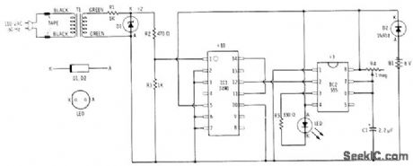
AUDIO_TO_DC_CONVERTER_CIRCUIT
Published:2009/7/12 22:38:00 Author:May

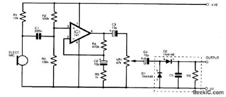
The circuit diagram for the audio input module, which produces a dc output voltage relative to the input signal amplitude. (View)
View full Circuit Diagram | Comments | Reading(1696)
8_BIT_BINARY_TO_DECIMAL_CONVERTER
Published:2009/7/12 22:37:00 Author:May
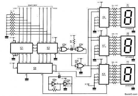
The decimal value of the eight input lines is displayed on three seven-segment displays. Although chips exist to perform this function for single displays, none include the possibility of displaying numbers greater than 9. No EPROM is necessary in this design. It operates by using two synchronized counters, one that generates an 8-bit binary output, and a second that drives the display. If the display is updated only when the binary counter is at the same value as the input, then the display will show the decimal value of the input. IC4 is the binary counter, and IC6 to IC8 form the display/counter section. IC5a and IC5b form the astable, which clocks both counters at 5 kHz.The minimum display refresh rate is, therefore, 20 times per second, IC1 and IC2 are two 4-bit comparators, ganged to form an 8-bit comparator. This compares the output of the binary counter (IC4) with the binary input taken from the circuit under test. Resistors RI to R8 pull down the input lines to prevent them from floating when no input is connected. When the comparator inputs are equal, pin 6 of IC2 goes high, triggering the monostable (IC3ab), which outputs a brief pulse. This latches the value of the display counters (IC6 to IC8) to the display. When IC4 reaches avalue of 256, the link between pins 11 and 12 resets the chip, and this resets the display counter also. (View)
View full Circuit Diagram | Comments | Reading(8664)
LIQUID_DENSITY_GAGE
Published:2009/7/12 22:36:00 Author:May

Peltier-effect semi-conductor thermoelements maintain uniform cooling temperatures required for accurate specific gravity measurements. Null-position detecting circuit uses differential transformer to sense position of movable core at end of float.-C. W. Hargens, Semiconductors Cool and Control Density Gage, Electtonics, 31:49, p 80-8l. (View)
View full Circuit Diagram | Comments | Reading(1115)
800_W_TRIAC_DIMMER
Published:2009/7/12 22:34:00 Author:May
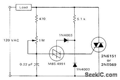
Simple circuit uses Motorola MBS-4991 silicon bilateral switch to provide phase control of triac. 1-megohm pot varies conduction angle of triacfrom0o to about 170o, to give better than 97% of full power to load at maximum setting. Conduction angle is the same for both half-cycles at any given setting of pot.-- Circuit Applications for the Triac, Motorola, Phoenix, AZ, 1971, AN-466 p 5. (View)
View full Circuit Diagram | Comments | Reading(2012)
LINEAR_DAC_WITH_NONLINEAR_OUTPUT
Published:2009/7/12 22:34:00 Author:May
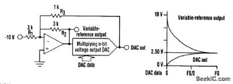
When controlling a nonlinear device, such as an incandescent lamp, it is desirable to have fine resolution at the high end, where a small change in current can cause a large change in brightness.At the low end, coarser resolution is quite adequate. Using the circuit shown, any desired compression can be produced using just about any multiplying DAC. A negative 10-V reference is fed through R1 to inverting amplifier A1, which has an initial gain set to unity by R2. A1's output supplies a positive variable reference to the DAC. The DAC output provides additional feedback through R3, reducing the amplifier's gain as the DAC data increase. The variable reference is gradually reduced so that each step is progressively smaller than the one before. With the values shown, as the DAC data approaches full-scale; the reference approaches 1/4 of its original value. This produces output with four times as much resolution at the high end as at the low end. By decreasing the value of R3, greater compression and higher resolution can be achieved. The variable-reference output also can be useful in some applications. (View)
View full Circuit Diagram | Comments | Reading(835)
15_V_FOR_VTVM
Published:2009/7/12 22:33:00 Author:May
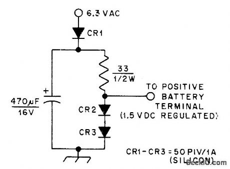
Simple rectifier circuit replaces battery in vacuum-tube voltmeter. Provides good regulation and eliminates need for frequent battery replacement. Remove battery before using supply. AC source can be 6.3-V secondary of filament transformer or terminals of 6.3-V pilot lamp in any AC equipment.-P. Alexander, Battery Replacement Circuit for VTVM, QST, Jan. 1976, p 42-43. (View)
View full Circuit Diagram | Comments | Reading(830)
MAX667 application circuit diagram
Published:2011/7/20 5:22:00 Author:nelly | Keyword: application
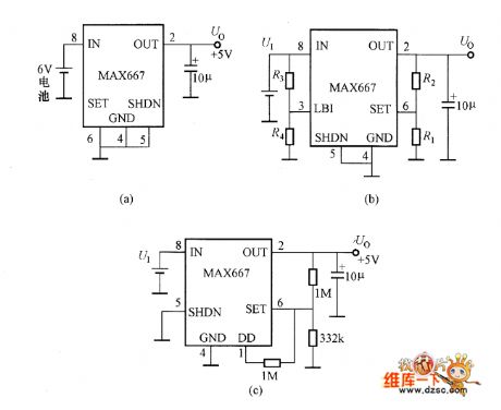
View full Circuit Diagram | Comments | Reading(939)
Discharge type single trigger timing circuit formed by PUT
Published:2011/8/2 5:14:00 Author:Nancy | Keyword: Discharge type, single trigger , timing
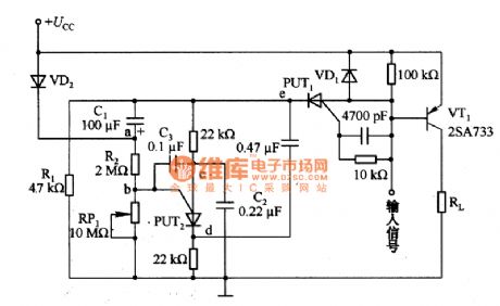
Figure 1 is the discharge type single trigger timing circuit formed by PUT. When there is no input signal, PUT1 cuts off, and so does the transistor VT1. At this time, C1 charges to the power supply voltage Ucc. If we add the input signal, PUT1 and VT1 conduct, current flows through the load RL. At the same time, the potential of point a is two times of the power supply voltage Ucc, C2 and C3 charge to the power supply voltage Ucc. From this time, C1 discharges through R2 and RP1, then the potential of point a drops slowly. After reaching the set time, if the potential of point b is lower than that of point c, then PUT conducts.
(View)
View full Circuit Diagram | Comments | Reading(584)
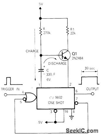
Long time delay circuit formed by the power MOSFET
Published:2011/7/26 10:06:00 Author:Nancy | Keyword: Long time delay, power MOSFET
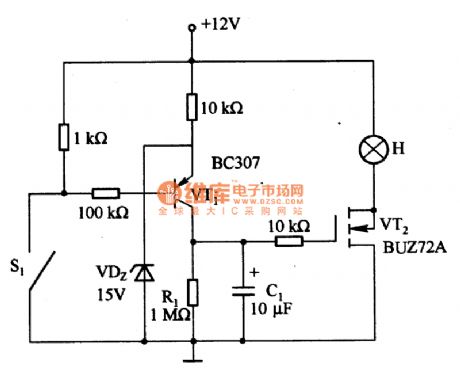
Figure 1 is a long time delay circuit formed by the power MOSFET. The grid input impedance of the power MOSFET is very high, so it is easy to choose the resistor and capacitor with large grid time constant. When the gate opens, the gate control switch S1 conducts, the base of VT1 is low level and in the conduction state, so the grid of the power MOSFET (VT2) is high level and conducts, the indoor light H is lit up. When the gate is closed, the gate control switch S1 disconnects, the base of VT1 is high level and cut off. However, the time constant formed by the R1 and C1 make VT2 conduct for lOs, which keeping the grid voltage of VT2 higher than threshold voltage. With the discharge of C1, the grid voltage of VT2 reduces and cuts off, the indoor light H burns out. (View)
View full Circuit Diagram | Comments | Reading(1988)
AFC varactor diode circuit diagram in this oscillator
Published:2011/7/20 4:55:00 Author:nelly | Keyword: AFC varactor diode, oscillator
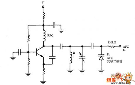
View full Circuit Diagram | Comments | Reading(2199)
BAlTERY_SAVER
Published:2009/7/12 22:30:00 Author:May
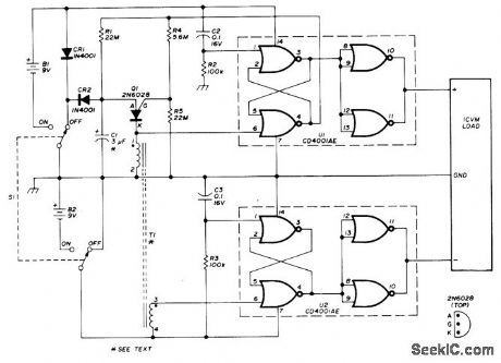
Tums off battery-powered IC VTVM automatically about 3.5 min aftertuning on with S1, to prolong battery life even though user forgets to tum off instrument. Circuit can be retriggered at any time in timing cycle by switching S1 off and then on again. Q1 is programmable UJT that drives latch using two gates of CD4001AE quad N0R gate U1. With pin 3 high and pin 4 low, timing circuit and load are both turned off; battery drain by U1 is then only 0.001 μA. Values of R1 and C1 determine time interval, T1 is air-core pulse trans-former having 600 tums (No. 36 to 401 enamel for primary and same number wound over primary for secondary.-R. Hardesty, Tum-Off Timer for Portable Equipment, Ham Fladio,Sept. 1976, p 42-44. (View)
View full Circuit Diagram | Comments | Reading(794)
Automatic trace phase shifting 90 circuit diagram
Published:2011/7/26 9:49:00 Author:Nancy | Keyword: Automatic trace, phase shifting
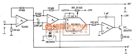
Figure 1 is a automatic trace phase shifting 90 circuit diagram. In the circuit, A1 is a buffer amplifier, which can amplify the input signal below 1 V into several volts. A2 is a phase shifting circuit with stable gain, the amplitude of the output signal is not relevant to the input frequency, it only changes the phase, so it is also called all pass filter.
The necessary condition to get 90 ° phase difference is RG=1/2πfC1, here we use servo circuit to control the RG. The synchronous detection circuit is formed by the analog multiplier, the output Uo of the synchronous detection circuit is equal to Ucosφ under the condition of 90° phase detection, which means it is not relevant to the amplitude of the input signal, the output Uo is equal to zero as long as the φ is equal to 90°. The integrator is also a servo circuit which uses VT1 to increase the output current. (View)
View full Circuit Diagram | Comments | Reading(658)
The adjustable Pulse signal source circuit with frequency and pulse width(CD4011)
Published:2011/8/4 8:10:00 Author:nelly | Keyword: Pulse, signal source, frequency, pulse width
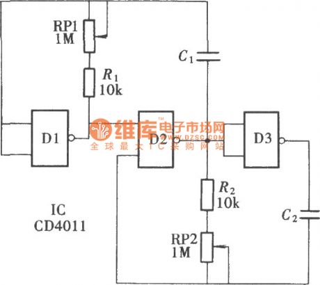
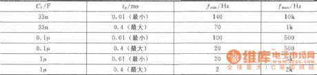
The signal pulse width of the general pulse generator will change with the oscillation frequency, when it is changing its oscillation frequency. Conversely, when the pulse needs to be changed, the oscillation frequency will also change. This circuit can make the pulse width of the pulse and the frequency change independently, so they will not influence each other, the circuit is as shown..
The table of oscillation frequency and pulse width:
(View)
View full Circuit Diagram | Comments | Reading(825)
90°phase separation circuit
Published:2011/7/26 9:25:00 Author:Nancy | Keyword: phased separation
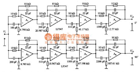
Figure 1 is the 90°phased separation circuit. It is a phase separation circuit formed by two circuits with the output phase difference keeping the same, it is used as a standby circuit of the variable frequency two phase oscillator or the basic signal source of the two phase lock-in amplifier. The circuit will offset 90 ° phase frequency into 8 sections, which are: f1=331.7KHz,f2=37.92KHz,f3=7.5799KHz,f4=1.4115kHz,f5=90.62kHz,f6=16.875KHz,f=3.372KHz,f=0.38561KHz. (View)
View full Circuit Diagram | Comments | Reading(971)
30_s_NONRETRIGGERABLE
Published:2009/7/12 22:28:00 Author:May
With values shown, rnono IC gives delay period of 30 s after triggering by input pulse and ignores other input pulses during timing period. Delaytimein seconds is RC/3, where R is in ohms and C in farads. Delay can be reduced to as little as 10ms by reducing R to 30 kilohms and C to 1 μF. Maximumdelay is about 1 min, with 560 kilohms for R.-F. R. Shirley, Thirty-Second Timer Uses IC One-Shot, EDNIEEE Magazine, Jan. 1, 1972, p 73-74. (View)
View full Circuit Diagram | Comments | Reading(674)
1_s_H_16_H_PRECISION
Published:2009/7/12 22:26:00 Author:May
Accuracy is comparable to that of 60-Hz power-line frequency. After Fladio Shack 276-561 6-V zener divides powerline frequency by 2, 7490 decade counter provides division by 10 to give 3 Hz. 555 timer connected as mono MVBR is then adjusted with R4 to divide by 3. LED then flashes at precise 1-s intervals, staying on about 100 ms, T1 is 6.3-V filamenttransf ormer.-F. M. Mints, Integrated Circuit Projects, Vol. 5, Radio Shack, Fort Worth, TX, 1977, 2nd Ed., p 21-29. (View)
View full Circuit Diagram | Comments | Reading(1217)
| Pages:191/471 At 20181182183184185186187188189190191192193194195196197198199200Under 20 |
Circuit Categories
power supply circuit
Amplifier Circuit
Basic Circuit
LED and Light Circuit
Sensor Circuit
Signal Processing
Electrical Equipment Circuit
Control Circuit
Remote Control Circuit
A/D-D/A Converter Circuit
Audio Circuit
Measuring and Test Circuit
Communication Circuit
Computer-Related Circuit
555 Circuit
Automotive Circuit
Repairing Circuit