
Index 182
DOUBLE_INTEGRATOR
Published:2009/7/16 4:06:00 Author:Jessie
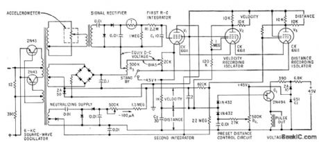
Used to measures distances up to 150 feet, from information supplied by slide-wire accelerometer. Transistor operates as voltage trip, providing output pulse when distance reaches preset value. Two other tubes provide velocity and distance information for recorder.-T. R. Nisbet, Double Integrator Finds Distance, Electronics, 32:21, p 64-66. (View)
View full Circuit Diagram | Comments | Reading(1009)
10_W_DUMMY_LOAD
Published:2009/7/13 3:54:00 Author:May
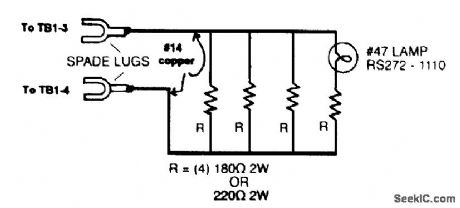
This dummy load was intended for tune-up of a 10-W CW ham rig. It should be useful for general-purpose applications in the HE range. The spade lugs shown can be replaced with a UHF connector for more versatility. The lamp acts as a relative power indicator. (View)
View full Circuit Diagram | Comments | Reading(774)
ODD_EVEN_LOGIC
Published:2009/7/16 4:06:00 Author:Jessie
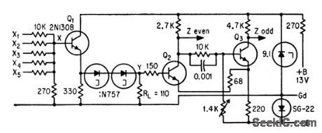
Accepts lye binary inputs and produces signal at either of two outputs according to whether sum of inputs is even or odd. Schmitt trigger is used between tunnel diodes and load to boost output voltage to 9 v.-W. H. Ko, Unique Tunnel-Diode Circuit Performs Odd-and-Even Logic, Electronics, 35:42, p 61-62. (View)
View full Circuit Diagram | Comments | Reading(1019)
800_MHz_ANTENNA
Published:2009/7/13 3:53:00 Author:May
This simple quarter-wave antenna can improve performance on the 800-MHz band and can be built in just a couple of hours. (View)
View full Circuit Diagram | Comments | Reading(769)
TRANSISTOR_COUPLED_NAND_NOR_GATE
Published:2009/7/16 4:05:00 Author:Jessie

Coupling transistor Q3 feeds its base current into base of inverting transistor Q2 when gate Q1 is cut off. When Q1 is saturated, coupling transistor Q3 clamps base of Q2 to low voltage. Logic swing of 0.4 v occurs at high speed.-A. E. Skoures, Choosing Logic for Microelectronics, Electronics, 36:40, p 23-26. (View)
View full Circuit Diagram | Comments | Reading(695)
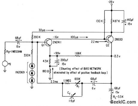
COMPENSATED_R_C_INIEGRATOR
Published:2009/7/16 4:05:00 Author:Jessie
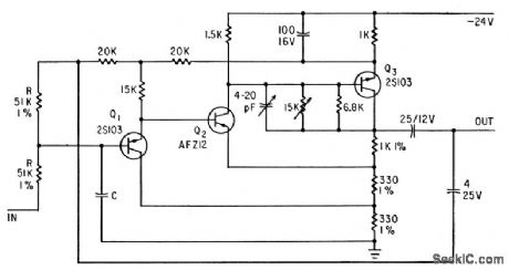
Overshoot is less than 2% at 3 db down for band-width of 20 Mc.-S. Berglund and S. Westerlund, Probes for Plasma Research with Wideband Integrators, Electronics, 35:24, p 44-45. (View)
View full Circuit Diagram | Comments | Reading(639)
INFINITE_INPUT_RESISTANCE
Published:2009/7/13 3:53:00 Author:May
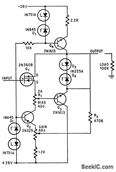
Uses metal oxide semiconductor field effect transistor as buffer to give input impedance of 1015 ohms.Amplifer gain is unity within 0.1% for 100K load. When adjusted, output equals input within 10 my over allowable range of 10 v above or below ground.-A. D. Delagrange, Amplifier Provides 1015-Ohm Input Resistance, Electronics, 39:17, p 99. (View)
View full Circuit Diagram | Comments | Reading(777)
COMPUTER_FOR_SIX_BIT_BINARY_OUTPUT
Published:2009/7/16 4:04:00 Author:Jessie
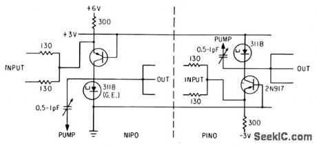
Pumped tunnel-diode-transistor logic at 300 Mc converts outputs of converter subchannels into time series of six bits. In nipo element, one or more negative pulses at input in.hibits positive-going pulse at output; other element operates at opposite half-cycles at pump source and gives opposite action.-H. R. Schindler, Semiconductor Circuits in c UHF Digital Converter, Electronics, 36:35, p 37-40. (View)
View full Circuit Diagram | Comments | Reading(753)
BASIC_VACUUM_TUBE_REGENERATIVE_DETECTOR
Published:2009/7/13 3:52:00 Author:May
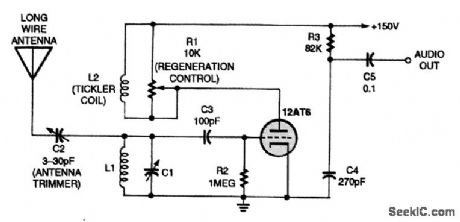
The traditional tube-based regenerative receiver is essentially an Armstrong RF oscillator with variable feedback that is connected to an antenna and a resonant circuit. C1 is usually a 140-pF variable capacitor, and L1 and L2 are wound on a plug-in coil form, with L2 typically having 10 to 20 percent of the turns on L1 and wound next to the cold side of L1. The inductance depends on the desired frequency range, but 150 kHz to about 18 MHz is typical for this circuit. (View)
View full Circuit Diagram | Comments | Reading(1741)
XENON_STROBE
Published:2009/7/13 3:52:00 Author:May
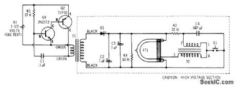
Two- transistor oscillator generates pulses at about 500 Hz for step-up by 300-mA filament transformer T1 (Radio Shack 273-1384) to charge storage capacitors C2 and C3, which are 250-V electrolytics. Simultaneously, C4 is charged through R2. After allowing sufficient time for capacitors to charge,S1 is pressed to discharge C4 through 272-1146 flashtube trigger transformer T2, which steps up voltage pulse to about 4000 V for ionizing gas in 272-1145 xenon flashtube FT1. C2 and C3 now discharge through ionized gas to produce brilliant flash of white light lasting only a few microseconds, as required for photography of objects moving at high speed. Circuit may require two cells in series for reliable operation.-F. M.Mims, Transistor Projects, Vol. 3, Radio Shack, Fort Worth, TX, 1975, p 49-60. (View)
View full Circuit Diagram | Comments | Reading(3242)
UNDERCOVER_SCANNER_ANTENNA
Published:2009/7/13 3:51:00 Author:May
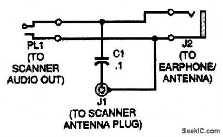
The figure shows the schematic for the antenna circuit. Because the circuit is passive.no power supply is needed. Plug PL1 connects to the audio output or earphone jack of a scanner. The audio signal is then fed to J2, the earphone/antenna jack of the circuit. A 0.1-μF capacitor, C1, connects the center ( hot ) terminal of J2 to a BNC jack, J1. When an earphone is plugged into J2, C1 feeds RE from the earphone wire to the front end of the scanner, through J1, without directly connecting the audio circuit to the receiver. An earphone connected to J2 will therefore both provide audio and act as anantenna.
(View)
View full Circuit Diagram | Comments | Reading(955)
QUADRATURE_DETECTOR_DESIGN
Published:2009/7/13 3:51:00 Author:May
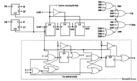
One common electrical requirement when dealing with motion control is to monitor the angular position of a rotating object.Quite often, an optical encoder is attached to a rotating shaft, and the encoder's quadrature outputs provide angular displacement information. The key is to turn those quadrature signals into clock pulses, and then into a displacement count that's useful for your application. This circuit requires a reset as well as a clock for sampling the input data. The clock frequency needs to be adjusted to guarantee at least one rising clock edge for each input state change. The circuit takes a set of quadrature signals (CHA, CHB), samples them with CLKIN, and generates output clock pulses (UP or DN) for each input state change. The up/down output clock pulses then can be fed directly into 74XX193 counters as the up and down clocks. If CLKIN is synchronized to external timing, the 193 ripple counter's output can be latched out of phase with the updates to ensure stable counter values. The timing diagram shows the internal functionality of the design. Intervals 1 to 5 illustrate the reset function, which blanks startup instability conditions.Intervals 5 through 12 show timing for a jitter pulse that's been sampled. Interval13 depicts a jitter pulse that missed being sampled and, therefore, caused no change in the output. The remaining intervals illustrate complete cycles for each direction of motion. (View)
View full Circuit Diagram | Comments | Reading(2521)
40_m_LOOP_ANTENNA
Published:2009/7/13 3:50:00 Author:May
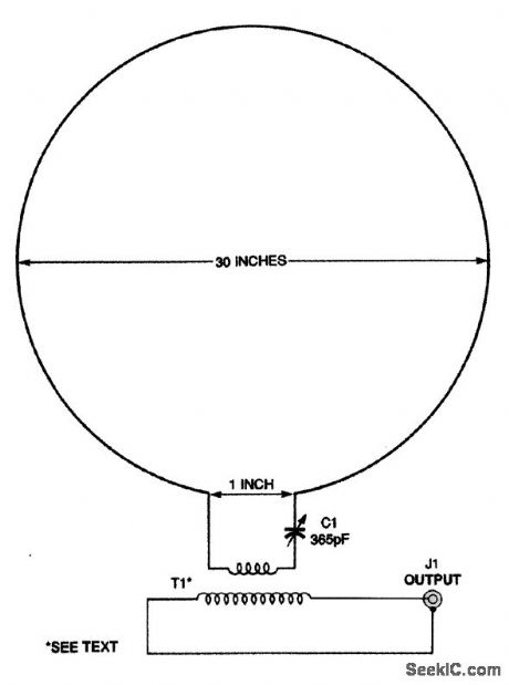
A cliff-dweller's dream, this 40-m loop can get apartment-based hams on the air. It also makes a great receiving antenna. The matching transformer, T1, is wound on T50-2 toroid core. The primary consists of 4 turns of 18-gauge enameled copper wire, and the secondary consists of 12 turns of 20-gauge enameled copper wire. Close-wind the secondary and the primary, and make sure that the two windings do not overlap. (View)
View full Circuit Diagram | Comments | Reading(2453)
12_LED_SEQUENTIAL_DRIVER
Published:2009/7/13 3:49:00 Author:May
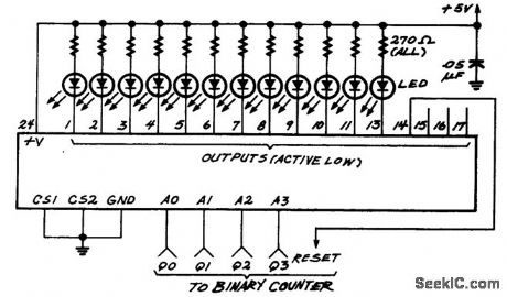
A demultiplexer selects a different LED for each binary number at its input. The counter resets after a count of 12. (View)
View full Circuit Diagram | Comments | Reading(701)
TIMER_SWITCH_OFF_FOR_ENLARGER
Published:2009/7/13 3:46:00 Author:May
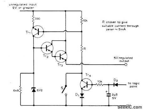
Circuit shows power supply designed to operate digital exposure timer using TTL. Since timer logic is needed only when enlarger lamp is on, power supply circuit will be turned off automatically when timer goes low and turns off enlarger lamp at end of exposure, Switch S is closed when timer cycleis activated, setting timer out-put at 5 V and turning on lamp. Transistor and diode types are not critical, Since D2 is con-netted to logic point of timer, power supply re-mains on when S is released, until completion of timer cycle.-E. R. Rumbo, Automatic Switch-Off Power Supply, WI'reless World, Feb.1976, p 77. (View)
View full Circuit Diagram | Comments | Reading(868)
R_C_SERVO_DRIVER_CIRCUIT
Published:2009/7/13 3:46:00 Author:May
The circuit shown produces the necessary pulse signal to drive R/C servos through a 90°range by adjustment of the pot R2. (View)
View full Circuit Diagram | Comments | Reading(933)
450_MC_R_F_FOR_AERONAUTICAL_BAND
Published:2009/7/13 3:46:00 Author:May
Common-base configuration gives slightlymore power gain at this frequency that common-emitter circuit,Power gain is 20 db,noise figure 4.5 db, and bandwidth 10 Mc,-Texas instruments Inc., sond-State Communications,McGraw-Hill, N,Y., 1966, P 298. (View)
View full Circuit Diagram | Comments | Reading(667)
HIGH_INPUT_IMPEDANCE_FROM_100_CPS_TO_230_KC
Published:2009/7/13 3:43:00 Author:May
For transducers requiring input impedance above 1 meg. Requires only single Power supply, for direct coupling of low-level high-impedance sources. Voltage gain is stable within 0.05 db of 20 db from -25 to +125℃. Power gain is 46 db and power consumption is only 65 mw.-Texas Instruments Inc., Solid-State Communications, McGraw-Hill, N.Y., 1966, p 294. (View)
View full Circuit Diagram | Comments | Reading(614)
MAJORITY_DECISION
Published:2009/7/16 4:03:00 Author:Jessie
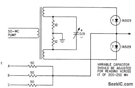
Balanced-pair tunnel-diode arrangement with phase-locked tank serves as gale operating on 50-Mc pump.-F. leary, Computers Today, Electronics, 34:17, p 64-94. (View)
View full Circuit Diagram | Comments | Reading(596)
DOUBLE_BALANCED_MIXER
Published:2009/7/16 4:03:00 Author:Jessie
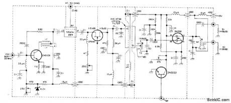
Uses grounded-gate CP643 preamp having high dynamic range,2N5109 oscillator injection amplifier, and 3N200 IF amplifier in combination with Minilabs SRA3H double-balanced mixer. Third-order intercept point is +30 dBm. Oscillator requirementis -1 to +2 dBm (200 to 280 mV across 50 ohms) AGC range is greater than 50 dB Levels shown in parentheses are for 0 dBm (224 mV) at input and zero AGC voltage.-U. L. Rohde, High Dynamic Range Receiver Input Stages, Ham Radio, Oct. 1975, p 26-31. (View)
View full Circuit Diagram | Comments | Reading(6603)
| Pages:182/471 At 20181182183184185186187188189190191192193194195196197198199200Under 20 |
Circuit Categories
power supply circuit
Amplifier Circuit
Basic Circuit
LED and Light Circuit
Sensor Circuit
Signal Processing
Electrical Equipment Circuit
Control Circuit
Remote Control Circuit
A/D-D/A Converter Circuit
Audio Circuit
Measuring and Test Circuit
Communication Circuit
Computer-Related Circuit
555 Circuit
Automotive Circuit
Repairing Circuit