
Index 200
DIODE_AND_FET_LEAKAGE
Published:2009/7/11 1:44:00 Author:May
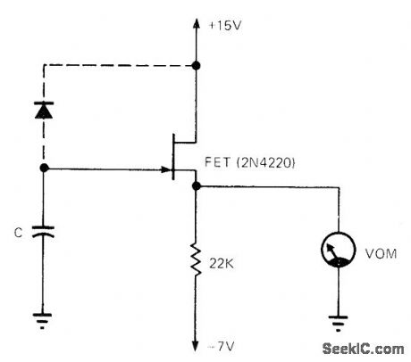
FET under test is connected with 22k resistor as source follower, with capacitor C across input from gate to ground. Leakage of FET charges capacitor at rate directly proportional to leakage and inversely proportional to capacitance. With 0.01 μF for C, each volt of change across C indicates stored charge of 10-8 coulomb. This can be interpreted as current in amperes if time for voltage on capacitor to rise 1 V is measured with stopwatch or timer while watching voltmeter. To test diode, connect as shown by dashed line and use good FET in circuit as shown. Article gives design equations; if voltage across C rises 1 V in 38.7 s, leakage current is 0.258 nA.-D. Dilatush, Leakage Testing of Diode and JFETs, EDNMagazine, May 5, 1973, p 72-73. (View)
View full Circuit Diagram | Comments | Reading(843)
TWO_PHASE_CLOCK_FOR_8080_1
Published:2009/7/11 1:43:00 Author:May
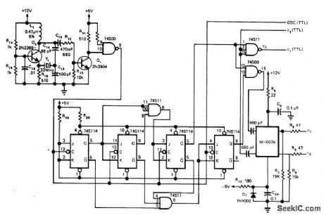
Typical clock design for Intel 8080 microprocessor system uses carefully designed logic sequence and level translation in combination with 32-MHz crystal to generate two-phase 12-V clock waveform.-S. G. Brannan, μP Clock Generators-Buy or Build? EDN Magazine,Sept 20,1975,p 53-55. (View)
View full Circuit Diagram | Comments | Reading(2565)
TWO_SPEED_CLOCK
Published:2009/7/11 1:42:00 Author:May
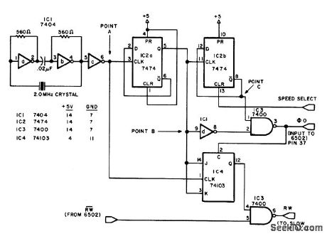
Creates alternative slow clock cycle for MOS Technology 6502 processor on KIM-1 microcomputer card under eontrol of SPEED SELECT line generated by slow memories. Control logic of 0 gives fast cycles, while logic 1 gives slow cycles. Processor cycle is maintained for 1 ps for fast memory access, but cycle is automatically stretched to 2μs for slower 2102s.-Y. M. Gupta, True Confessions: How I Relate to KIM, BYTE, Aug. 1976, p 41-48. (View)
View full Circuit Diagram | Comments | Reading(983)
TWO_INVERTER_COLPITTS
Published:2009/7/11 1:40:00 Author:May
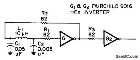
Simpie low-cost clock uses two inverters in LC circuit. G1 operates as Colpitts oscillator, with C1 setting feed-back Ievel and L1-C2 setting frequency. Low DC resistance path through R1, R2, and L1 provides high negative DC feedback around G1 and biases it into Iinear region. G2 squares output of G1 to appropriate TTL levels. For values shown, output period is 1.2 μs and rise and fall times are under 20 ns.-C. A. Herbst, TTL Inverter Makes Stable Colpitts Oscillator, EDN|EEE Magazine, May 15, 1971, p 50. (View)
View full Circuit Diagram | Comments | Reading(1820)
SIGNAL_INJECTOR
Published:2009/7/11 1:40:00 Author:May
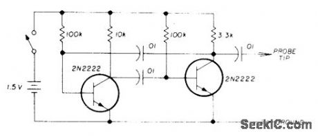
Circuit is basically 1-kHz MVBR having high harmonic output through 50 MHz. Used with signal tracer for troubleshooting audio equipment. Practically any NPN transistors can be used Article gives troubleshooting techniques for all types of equipment.-M,James,Basic Troubleshooting,Ham Radio,Jan,1976, p54-57. (View)
View full Circuit Diagram | Comments | Reading(0)
TWO_PHASE_CLOCK_FOR_8080
Published:2009/7/11 1:34:00 Author:May
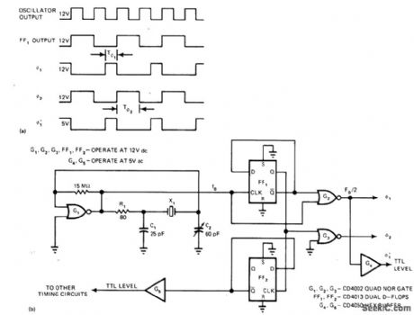


Crystal oscillator opetating at twice desired dock frequency uses pi network R1-C1-X1-C2 providing 180°phase shift required for positive feedback to input of oscillator G1. D flip-flop FF1 in divide-by-2 configuration generates one phase, while NOR gate G2 generates other phase from basic oscillator by masking out every other cycle. G3 merely provides enough propagation delay on second phase to prevent overlap with first phase. Crystal should be below 3 MHz.-D. M.Risch, 8080 CMOS Clock Uses Two IC's, EDN Magazine, Jan. 5, 1977, p 50. (View)
View full Circuit Diagram | Comments | Reading(2268)
CRYSTAL_CONTROLLED_MVBR
Published:2009/7/11 1:34:00 Author:May
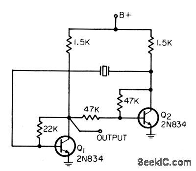
Simplicity and stability make circuit useful as system clock.Will oscillate at 1 Mc over supply voltage range of 2 to 30v.Output is rounded square wave,at any frequency from 3 kc to 10 Mc depending on crystal used.-J. Freeman, Crystal Controlled Multivibrator, EEE,13:6, p65. (View)
View full Circuit Diagram | Comments | Reading(796)
25_kHz_CLOCK
Published:2009/7/11 1:32:00 Author:May
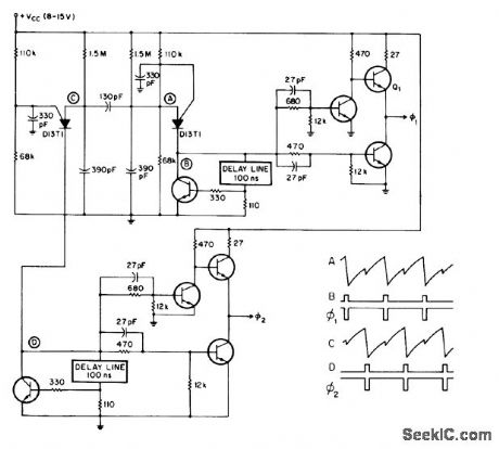
Requires only 3-mW power to generate fast 15-V two-phase rectangular pulses with 100-ns widths and 20-ns rise and fall times. Suitable for many MOSFET shift regiters. Uses two D13T1 programmable UJT oscillators, each having four-transistor driver stage using 2N2369 transistors. Oscillators are crosssynchronized by 130-pF capacitor. Timing and bias networks of UJTs set pulse repetition frequency.-G. A. Altemose, Low-Power Two-Phase Clock, EDN|EEE Magazine, May 15, 1971, p 49. (View)
View full Circuit Diagram | Comments | Reading(888)
SENSOR_SWITCH_AND_CLOCK
Published:2009/7/11 1:16:00 Author:May
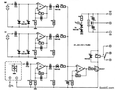
One TL084 IC and an old quartz watch enable the construction of a deluxe on/off switch. Two of the four op amps contained in the TL084 (A1 and A2) are used to amplify the input signals from the sensors by one hundredfold (with the component values as shown in the diagram). Just touching the sensors with a finger causes a good 50-Hz input signal (hum). Notice that the amplification drops rapidly with rising fre-quency.Diodes D5 and D6 rectify (single-phase) the 50-Hz signal. Because the diodes are connected in anti-phase, touching the off sensor causes a positive potential across C10, whereas touching the on sen-sor produces a negative potential across C10.Op amp A4 is connected as an inverting bistable so that a negative potential across C10 causes relay Re1 to be energized. Because of feedback resistor R16, this state is maintained until the other sensor is touched.The relay can also be energized at a predetermined time with the aid of a quartz watch. The 1.2-V supply for the watch is derived from the voltage drop across diodes D9 and D10; it can be increased to 1.8 V by adding a third diode.The piezo buzzer in the watch is connected to the input of A3 via C5. As soon as the alarm goes off (the hour signal must be off), the voltage across C10 becomes negative, the relay is energized, and the load is switched on. The circuit, excluding the relay, draws a current of about 20 mA. (View)
View full Circuit Diagram | Comments | Reading(4967)
TREMOLO_CIRCUIT
Published:2009/7/11 1:14:00 Author:May
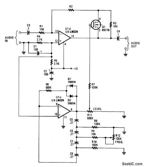
This circuit adds a VLF AM component to an audio signal. This effect is widely used in musical instru-ments. U1C, a phase-shift oscillator operating at a few Hz applies a signal to Q1, which modulates the gain of U1D. R11 varies the level of the effect, while R12 varies the frequency. (View)
View full Circuit Diagram | Comments | Reading(908)
TIME_OUT_CIRCUIT
Published:2009/7/11 1:11:00 Author:May
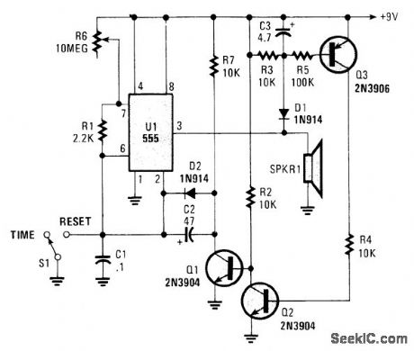
This circuit operatesin the astable mode and at the end of the first period (up to several minutes), itproduces a tone,When S1is placed h the time position,Q3 is cut off because pin 3 of U1 is high and D1 holds Q3in cutoff.Q2is off,and Q1is on,which grounds the negative end of D2 and C2,Therefore,C1and C2 are returned to ground.After a time of about 1.1 R6(C1 + C2),the timer cycle completes and pin 3 U1 goeslow,This turns on Q3 and Q2,cuts off Q1,and effectively disconnects C2.Now,the circuit oscillates with a period determined by,R7 and C1,because D2is forwardˉbiased. A toneis then generated and can be heard from SPKR1.Closing S2 resets the circuit. (View)
View full Circuit Diagram | Comments | Reading(771)
LONG_DURATION_TIME_DELAY
Published:2009/7/11 1:07:00 Author:May
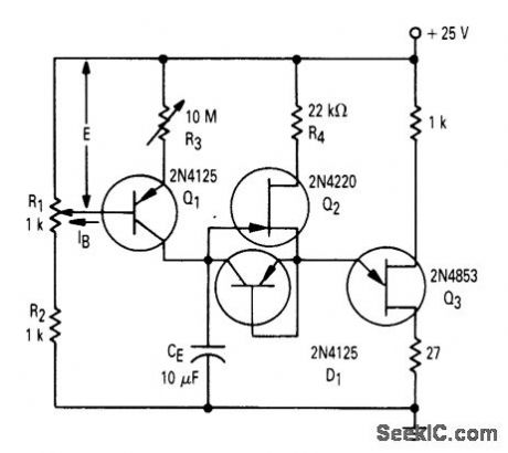
Transistor Q1 and resistors RI, R2, and R3 form a constant current source and the charge cur-rent might be adjusted to be as low as a few nanoamperes. This current would, of course, not be sufficient to fire the UJT where Ip=0.2 μA, unless the peak current was supplied from another source. Field-effect transistor Q2, acting as a source follower, supplies the current flowing into the emitter lead prior to firing and diode D1 provides a low-impedance discharge path for CE. D1 must be selected to have a leakage that is much lower than the charge current.Because IB is small, the delay time will vary linearly with R3. The voltage (E), applied across R3 and the base-emitter junction of Q1, is set by the variable resistor R1. Time delays up to 10 hours are possible with this circuit. Resistor R4, in series with the FET drain terminal, must be large enough not to allow currents in excess of IV to flow when the UJT is on. Otherwise, the UJT will not turn off and the circuit will latch up. (View)
View full Circuit Diagram | Comments | Reading(2425)
HIGH_ACCURACY_THERMOMETER
Published:2009/7/11 0:46:00 Author:May
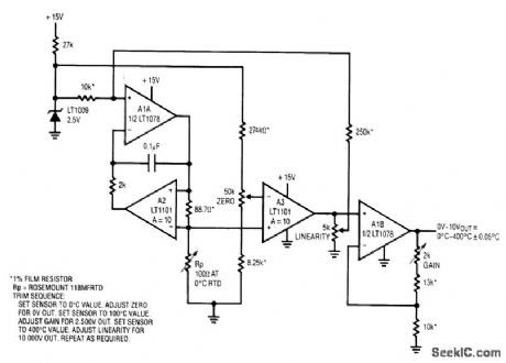
This circuit combines a current source and a platinum RTD bridge to form a complete high-accuracy thermometer. The ground,referred RTD sits in a bridge that is composed of the current drive and the LT1009 biased resistor string. The current drive allows the voltage across the RTD to vary directly with its temperature-induced resistance shift. The difference between this potential and that of the opposing bridge leg forms the bridge output. The RTD's constant drive forces the voltage across it to vary with its resistance, which has a nearly linear positive temperature coefficient. The nonlinearity could cause several degrees of error over the circuit's 0℃ -400℃ operating range.The bridge's output is fed to instrumentation amplifier A3, which provides differential gain, while simultaneously supplying nonlinearity correction. The correction is implemented by feeding a portion of A3's output back to A1's input via the 10- to 250-kΩ divider. This causes the current supplied to Rp to slightly shift with its operating point, compensating sensor nonlinearity to within ±0.05℃. A1B, provid-ing additional scaled gain, furnishes the circuit output.To calibrate this circuit, follow the procedure given in the diagram. (View)
View full Circuit Diagram | Comments | Reading(1043)
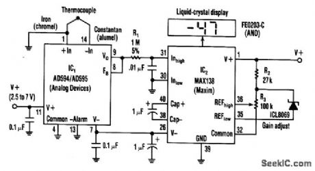
SINGLE_dc_SUPPLY_THERMOMETER
Published:2009/7/11 0:41:00 Author:May
Using a J-type thermocouple, this circuit can indicate temperatures from -350° to 400° with a 6-V supply or -50 to + 100° with a 3-V lithium battery. The AD954 produces 10 mV/°C output to the MAX 138 digital voltmeter chip, which drives the LCD display. (View)
View full Circuit Diagram | Comments | Reading(1423)
ELECTRONIC_THERMOMETER
Published:2009/7/11 0:39:00 Author:May
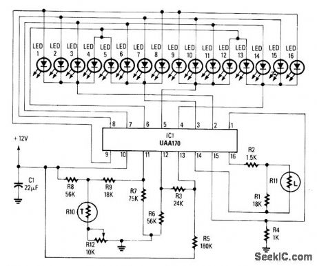
This thermometer uses an NTC thermistor (R10) to produce a dc voltage that decreases with tem-perature, to drive an IC that lights one of the 16 LEDs as a function of this voltage. R11 is a light-depen-dent resistor that adjusts the LED brightness as a function of ambient light. (View)
View full Circuit Diagram | Comments | Reading(0)
INEXPENSIVE_LINERA_THERMOMETER
Published:2009/7/11 0:39:00 Author:May
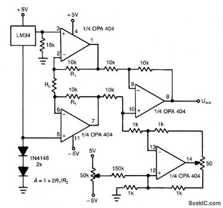
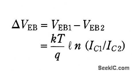
As a sensor in the design of this linear thermometer, the LM34 is used. The output is the difference between two base-emitter voltages vEB of two transistors operated at different collector-current densi-ties. The voltage difference (△VEB) is:where the current densities are IC1 and IC2,k is Boltzrnann's constant, and q is the electron charge. Because all factors, including the ratio IC1/IC2 are constant, the output of the LM34 (Nationgl Semiconduc-tor) is a linear function of T in the range over -50°to 300°F, which provides the output voltage of 10 mV/ °F with a max. nonlinearity of ±0.35°F.The output of the LM34 is amplified by a three-op-amp instrumentation amplifier. The fourth op amp gives the possibility to control the offset voltage of the amplifier. The gain A of the instrumentation amplifier can be set to any desired value by the choice of the resistance R2 only. (View)
View full Circuit Diagram | Comments | Reading(797)
TEMPERATURE_CONTROLLER_WITH_DEFROST_CYCLE
Published:2009/7/11 0:10:00 Author:May
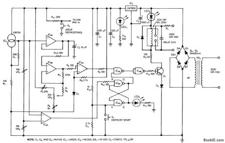
This temperature controller has a range of -50 to +150°C and permits defrosting. R7, VR3, and R8 set the controller's trip point. 51 initiates defrosting, S2 cancels defrosting. VR1 and VR2 set the defrost-temperature trip point.The LM134, IC1, is a thermal sensor. One section of IC3, a quad op amp, buffers the sensor's output. The other section func-tions as Schmitt trigger and buffer for the normal-cycle circuitry and as a comparator for the defrost-cycle circuitry. If you wish to control a heater rather than a refrigerator, omit the final inverter in Q1's base circuit. You must select LM7805s that have outputs between 4.95 and 5.05 V, or the circuit might not work. (View)
View full Circuit Diagram | Comments | Reading(1667)
lOO_KG_CLOCK_FOR_COUNTER
Published:2009/7/10 23:56:00 Author:May
Stable fixed-frequency Pierce oscillator becomes transistorized Clapp oscillator when crystcd is replaced by high-Q L-C tuner.-W Fryer,How to Design Low Cost Audio Filters,Elecltonics,32:15,p68-70. (View)
View full Circuit Diagram | Comments | Reading(680)
DRIVER_FOR_24_MOS_REGISTERS
Published:2009/7/10 23:56:00 Author:May
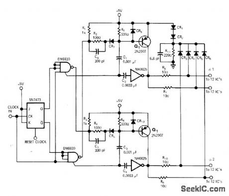
With input of clock pulses preshaped to width of about 150ns, circuit shown will generate 17-V,1.5-A clocksignal required for driving 1024-bit serial MOS memories or shift registers Article traces operation of circuit All diodes are 1N3064.-R. D. Hoose and G. L. Anderson, Clock Driver for MOS Shift Registers,EDN|EEE Magazine.Dec, 15, 1971, p 56-57. (View)
View full Circuit Diagram | Comments | Reading(692)
60_Hz_GLITCH_FREE_CLOCK
Published:2009/7/10 23:54:00 Author:May
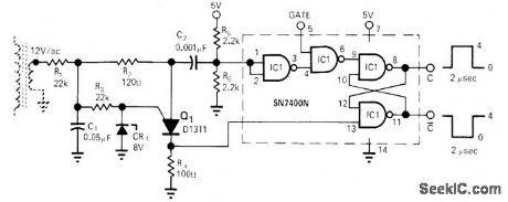
Circuit generates complementary gated 60-Hz dock pulses that are always wider than 2 μs, without glitches even if gate is enabled or disabled during clock pulse. Accuracy depends on stability of powerline frequency.-R. I. White, Gated 60 Hz Clock Avoids Glitches, EDN|EEE Magazine, Nov. 1, 1971,p 52. (View)
View full Circuit Diagram | Comments | Reading(677)
| Pages:200/471 At 20181182183184185186187188189190191192193194195196197198199200Under 20 |
Circuit Categories
power supply circuit
Amplifier Circuit
Basic Circuit
LED and Light Circuit
Sensor Circuit
Signal Processing
Electrical Equipment Circuit
Control Circuit
Remote Control Circuit
A/D-D/A Converter Circuit
Audio Circuit
Measuring and Test Circuit
Communication Circuit
Computer-Related Circuit
555 Circuit
Automotive Circuit
Repairing Circuit