
Measuring and Test Circuit
Index 76
BABY_MONITOR
Published:2009/6/23 3:31:00 Author:May
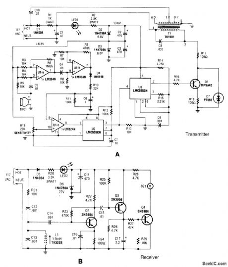
Transmitter operation. Operating power for the transmitter circuit is derived directly from the ac line. The dc power to operate the circuit is generated in two stages, one for an RE power-amplifier stage, and the second for the remainder of the circuit.
The ac line voltage is applied to D1 , which half-wave rectifies the ac input . The resulting dc voltage (approximately 30V under load) is fed across an RC filter (comprised of R1 and C1) and used to operate amplifier, Q1. The second stage of the power supply (composed of LED1, R2, D2, D3, C2, and C3, which forms a regulated +13.6-V, center-tapped supply) feeds the remainder of the circuit. LED1 is connected in series with R2 and is used as a visual power-on indicator for the transmitter.
An electret microphone element (MIC1) is used as the pick-up. The output of the microphone is ac coupled through C5 to UI-a (a noninverting op amp with a gain of about 100). The output of U1-a at pin 1 is ac coupled through C4 to the noninverting input of UI-b (which provides an additional gain of 48) at pin 5. The output of UI-b at pin 7 is then fed through D4 and RIO, and across R11 and C6 to the inverting input of UI-c which is biased to a positive voltage that is set by SENSITIVITY-control R19. This represents a threshold voltage at which the output of UI-c switches from high to low.
During standby, the output of UI-c at pin 8 is held at about 12 V when the voltage developed across C6 is less than the bias-voltage setting at pin 10. When a sound of sufficient intensity and du-ration is detected, the voltage at pin 9 of UI-c exceeds the threshold level (set by R19), causing UI-c's output at pin 8 at go low. That low is applied to pin 2 of U2 (a 555 oscillator/timer configured as a monostable multivibrator). This causes the output of U2 to go high for about one second, as de-termined by the time constant of R12 and C7. The output of U2 at pin 3 is applied to pin 4 of U3 (a second 555 oscillator/timer that is conftgured for astable operation, with a frequency of about 125 kHz). That causes U3 to oscillate, producing a near square-wave output that is used to drive Q1 into conduction. The output of Q1 is applied across a parallel-tuned circuit composed a T1's primary and C8. The tuned circuit, in turn, reshapes the 125-kHz signal, causing a sine-wave-like signal to appear across both the primary and the secondary of Tl.
The signal appearing at T1's secondary (about 1 or 2 V peak-to-peak) is impressed across the ac power line, and is then distributed throughout the building without affecting other electrical appli-ances connected to the line. Transient suppressor D7 is included in the circuit to help protect Q1 from voltage spikes that might appear across the power line and be coupled to the circuit through T1.
Receiver operation. Power for the receiver, as with the transmitter, is derived from a tradi-tional half-wave rectifier (D5). The resulting dc voltage is regulated to 27 V by D6 and R20, and is then filtered by C11 to provide a relatively clean, dc power source for the circuit. A light-emitting diode, LED2, connected in sGries with R20 provides a visual indication that the circuit is powered and ready to receive a signal.
The 125-kHz signal is plucked from the ac line and coupled through R21 and C12 to a parallel-tuned LO circuit, consisting of C13 and L1. That LO circuit passes 125-kHz signals while attenuating all others. The 125-kHz signal is fed through C14 to the base of Q2 (which is configured as a high-gain linear amplifier), which boosts the relatively low amplitude of the 125-kHz signal. The RE out-put of Q2 is ac coupled to the base of Q3 through C15. Transistor Q3 acts as both an amplifier and detector. Because there is no bias voltage applied to the base of Q3, it remains cut off until driven by the amplified 125-kHz signal. When Q3 is forward biased, its collector voltage rises.
Capacitor C16, connected across Q3's collector resistor, filters the 125-kHz signal so that it is essentially dc. When the voltage at the collector of Q3 rises, Q4 is driven into conduction. That causes current to flow into piezo buzzer BZ1, producing a distinctive audio tone that alerts anyone within earshot that the baby needs attention. (View)
View full Circuit Diagram | Comments | Reading(0)
MASTER_SLAVE_DEVICE_ERROR_CHECKER
Published:2009/6/23 3:30:00 Author:May
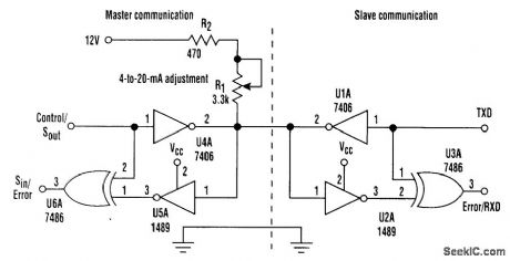
An error-check mechanism introduced into master and slave communication devices can indi-cate mismatches when both the master and slave start sending data simultaneously. The error ftag goes high and indicates a mismatch in the data.The master is the one that can interrupt the communication from a device at the other end and force it to listen. It does this forcing a low voltage level over the communication line by raising the control line to a high level. This inhibits data flow over the tines from the slave device. As a result, the slave turns into a listen mode(not a hardware feature, but rather incorporated in the software). The slave device can transmit the data after communication from the master device ceases. (View)
View full Circuit Diagram | Comments | Reading(0)
ROOM_MONITOR
Published:2009/6/23 3:17:00 Author:May
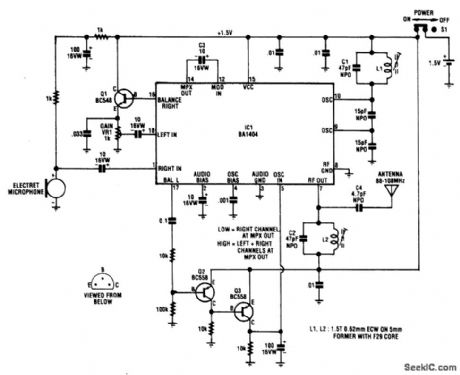
The circuit uses Q1 to buffer the right-channel balance output while Q2 and Q3 form a VOX circuit. When the signal level from the microphone goes high, the output of the VOX also goes high and the multiplexer inside IC1 switches the high-gain left-channel output through to a following buffer stage. This signal is then ac-coupled via C3 into an RE mixer stage and thence to an RF amplifier, which is tuned by C2 and L2. (View)
View full Circuit Diagram | Comments | Reading(0)
ac_POWER_LINE_MONITOR
Published:2009/6/23 3:07:00 Author:May
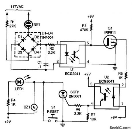
When the power-line voltage source fails,Q1 turns on,activates optoisolator U2, and triggers SCR1.For small SCRs,U1 might directly trigger SCR1. (View)
View full Circuit Diagram | Comments | Reading(0)
AUDIO_MIXER
Published:2009/6/23 2:56:00 Author:May
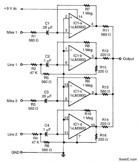
Designed around an LM3900 quad op amp, this mixer combines 2-line and 2-mike inputs and sums them at the output terminal. R7 through R10 can be changed to vary the gain (around +23 dB). (View)
View full Circuit Diagram | Comments | Reading(0)
The open-state level test circuit diagram indicated by lighting Dp decimal point
Published:2011/7/20 20:16:00 Author:Ecco | Keyword: open-state, level test , indicated , lighting, Dp decimal point
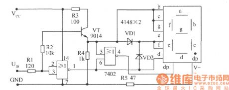
The open-state level test circuit diagram indicated by lighting Dp decimal point is shown as the chart. VT is conducted when it is in high level, it indicates H; VT is cut off when it is in low level, pin 1 of 7402 is in high level, it indicates L; when probe opens the circuit, pin 2,3 of 7402 are input high level, pin 1 outputs low level. At the same time, VT cuts off, pin 5 is pulled down in low level by R4, only pin 4 outputs high level to drive dp decimal point to emit.
(View)
View full Circuit Diagram | Comments | Reading(861)
LOW_NOISE_4_CHANNEL_GUITAR_MIXER
Published:2009/6/23 2:47:00 Author:May
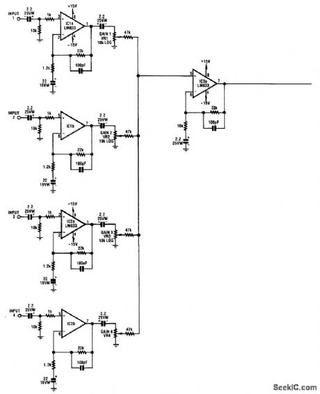
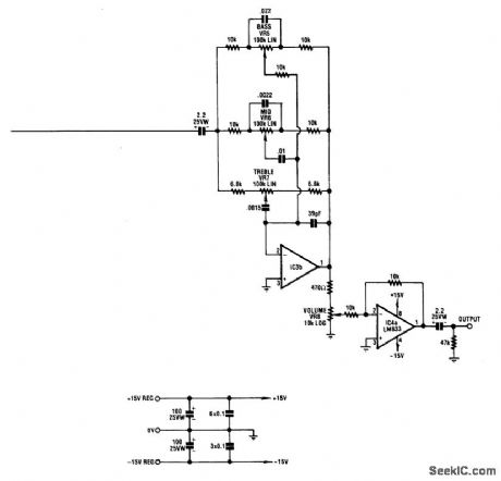
IC1-a,IC1-b,IC2-a,and IC2-b all function with a gain of about 19. Their outputs are mixed via the level-control pots and the resulting signal amplified by IC3-a and fed to tone-control stage IC3-b.Finally,the output from IC3-b is fed to unity gain buffer stage IC4-a via volume-control potgntiometer VR8. (View)
View full Circuit Diagram | Comments | Reading(1862)
INRUSH_CURRENT_LIMITER
Published:2009/6/23 2:40:00 Author:May
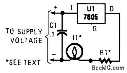
A 7805 can be configured as a constant-current regulator, to serve as an inrush current limiter. R1 will have 5V across it at all times so the total current through I1 will be 5 V/R1 + 5 mA, the 5 mA being the regulator operating current. In this case, R1 = 5 V/95 mA = 52.6Ω for I1 current = 100 mA. (View)
View full Circuit Diagram | Comments | Reading(0)
Simple 51 test board
Published:2011/7/25 3:01:00 Author:Ecco | Keyword: Simple, 51 , test board
It can complete the water lights directly, digital dynamic static display, small speakers sing, 24c02 read and write, keyboard control, serial communications test. (View)
View full Circuit Diagram | Comments | Reading(1559)
AUDIO_MEMO_ALERT
Published:2009/6/23 2:16:00 Author:May
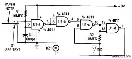
This device prevents paper notes and memos from being overlooked. A paper note placed be-tween two fingers made of a conducting material (metal or conductive plastic) breaks the circuit, al-lowing pair 1 of U1-a to go high. This causes U1-c & U1-d to act as an oscillator, pulsing piezo buzzer BZ1. (View)
View full Circuit Diagram | Comments | Reading(646)
HYDROPHONE
Published:2009/6/23 2:13:00 Author:May
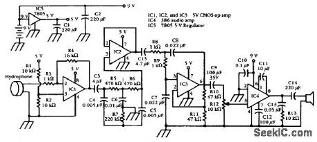
A commercially available hydrophone transducer is used in this system. The transducer is con-nected via a cable to the amplifier, which remains out of the water. The hydrophone should be suitably mounted for intended application. (View)
View full Circuit Diagram | Comments | Reading(3130)
AUDIO_MIXER
Published:2009/6/23 1:49:00 Author:May

The 741 op amp is used as a summing amplifier to combine several audio inputs. Overall gain is set by Rf. (View)
View full Circuit Diagram | Comments | Reading(0)
IN_LINE_WATTMETER
Published:2009/6/23 1:34:00 Author:May
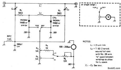
The circuit is not frequency sensitive. Its calibration will be accurate over a wide fre-quency spectrum, such as the entire amateur hf spectrum, if the values of L2, the voltage di-vider capacitors C1-2 and C3, and the resis-tances of RI-2 are chosen properly. R1-2 and CR1-2 should be matched for best results.Generally, R1-2 must be small compared to the reactance of L2 so as to avoid any significant effect on the L2 current which is induced by the transmission line current flowing through L1. The lower frequency limit of the bridge is set by the RI-R2/Ls ratio, and the cutoff is at the point where the value of RI-R2 becomes significant with reference to the reactance of L2 at that frequency point. (View)
View full Circuit Diagram | Comments | Reading(942)
RF_POWER_METER
Published:2009/6/23 1:32:00 Author:May
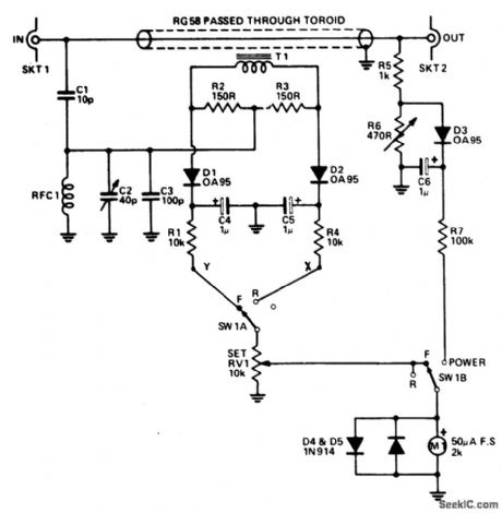
Reflectometer (SWR Power Meter) covers three decades-from 100 kHz to100 MHz. It can be constructed for rf powers as low as 500 mW or up to 500 watts. (View)
View full Circuit Diagram | Comments | Reading(6923)
HOME_SECURITY_MONITOR_SYSTEM
Published:2009/6/22 23:40:00 Author:May
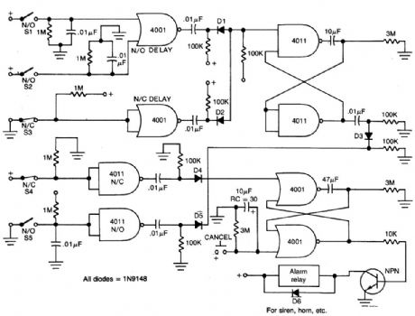
This circuit provides normally open (NO) and normally closed (NC) contacts S1, S2, and S3 to turn on the alarm after a 30 second delay. S4 and S5 operate instantly. The CANCEL switch resets the alarm. (View)
View full Circuit Diagram | Comments | Reading(778)
AUDIBLE_CONTINUITY_TESTER
Published:2009/6/22 23:35:00 Author:May
View full Circuit Diagram | Comments | Reading(0)
SIMPLE_AUDIO_VIDEO_CABLE_TESTER
Published:2009/6/22 23:34:00 Author:May
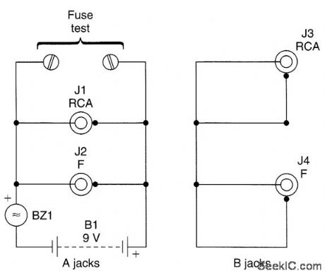
As simple as it looks, the audio/video cable tester tests cables while they are plugged in. You can flex them vigorously while listening to the built-in buzzer.Simply plug the ends of the cable in the appropriate jack. Only one end of the cable need be plugged in for a complete short test; the other end is left free. If the buzzer sounds, there is a short circuit somewhere in the cable. If nothing is heard, test for an intermittent short by flexing the cable several times, particularly in the plug area of both the free and plugged-in ends. (View)
View full Circuit Diagram | Comments | Reading(792)
ADJUSTABLE_CONTINUITY_TESTER
Published:2009/6/22 23:34:00 Author:May
A problem with most continuity testers is that the exact decision point (circuit resistance) be-tween continuity and open is indefinite. This circuit allows setting of this point to a known resistance between 1 and 50Ω. (View)
View full Circuit Diagram | Comments | Reading(1106)
TACHOMETER_DERIVED_FROM_BRUSHLESS_SHAFT_ANGLE_RESOLVER
Published:2009/6/22 23:26:00 Author:May
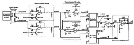
The tachometer circuit operates in conjunction with a brushless shaft-angle resolver. By performing a sequence of straight-forward mathematical operations on the resolver signals and utilizing a simple trigonometric identity, it generates a voltage pro-portional to the rate of rotation of the shaft.The figure illustrates an analog tachometer circuit that processes the input and output signals of a two-phase, brushless, transformer-type shaft-angle resolver into a signal with instantaneous amplitude proportional to the instantaneous rate of rota-tion of the shaft. The processing in this circuit effects a straightforward combination of mathematical operations leading to a fi-nal operation based on the well-known trigonometric identity [sin(x)]2 + [cos(x)]2 = 1 for any value ofx.The resolver is excited with a periodic waveform; a sinusoid is indicated in the figure, but a square, triangular, or other peri-odic waveform could be used instead. Thus, the two outputs of the resolver are k1 sin(ωt)sin(θ) and k1 sin(ωt)cos(θ), where k1 is a constant proportional to the amplitude of excitation, cot is 2nm the frequency of excitation, t is time, andθis the instantaneous shaft angle.The two outputs of the resolver are then processed, along with a replica of the sinusoidal excitation, by demodulators. These signals are then differentiated with respect to time in two differentiator circuits. Notice that dB/dt is the rate of change of the shaft angle and is the quantity that one seeks to measure.Next, a multiplier circuit forms a product of the demodulator and differentiator outputs proportional to sin(θ), and the prod-uct of the demodulator and differentiator outputs proportional to cos(θ), The output of the cosine multiplier is fed to a unit-gain inverting amplifier. (View)
View full Circuit Diagram | Comments | Reading(1863)
The miniature electron accounts price scale composed of S8 low price electron weigh chip
Published:2011/7/21 3:07:00 Author:Ecco | Keyword: miniature electron accounts price scale , electron weigh chip
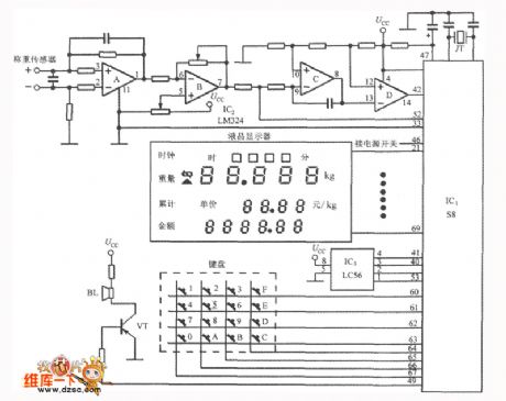
The S8, S9 are two kinds of electron weigh chip in low price, the common characteristics of two model can be summarized as they can directly drive liquid crystal display(LCD), and they can account price and weigh. It's suitable to constitute small scaled or miniature electronic scale. The telephone that is constituted a miniature electron to account price scale by the S8 is shown as chart. Only using 3 slabs of integrated circuits in the telephone:IC1(S8), IC2(four lucks put LM324), IC3(the 2 Kb E2 PROM chip LC56), the electron accounts all of the price scales to adopt a table put up component and measures the accuracy as 1%~0.5%, the volume is small, the cost is low, it's suitable quantity production.
Its main function is as follows: To account price and heavy, to accumulate times, to accumulate figure , display clock, the intelligence to cut of and select rangeabilities of 10 kg, 15 kg, 50 kg and 80 kg, to set null adjustment and null tracking, auto peeling, clear function, a prompt to error, overload indication, low -voltage indication. (View)
View full Circuit Diagram | Comments | Reading(630)
| Pages:76/101 At 206162636465666768697071727374757677787980Under 20 |
Circuit Categories
power supply circuit
Amplifier Circuit
Basic Circuit
LED and Light Circuit
Sensor Circuit
Signal Processing
Electrical Equipment Circuit
Control Circuit
Remote Control Circuit
A/D-D/A Converter Circuit
Audio Circuit
Measuring and Test Circuit
Communication Circuit
Computer-Related Circuit
555 Circuit
Automotive Circuit
Repairing Circuit