
Measuring and Test Circuit
Index 81
CRTSTAL_RADIO_DETECTOR
Published:2009/6/18 3:57:00 Author:May
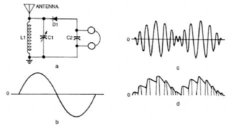
This is a crystal detector receiver with headphones (Fig. 26-13A), audio-frequency signal (Fig.26-13B), modulated signal (Fig. 26-13C), and a demodulated wave (Fig. 26-13D). (View)
View full Circuit Diagram | Comments | Reading(878)
15_kHz_TONE_DETECTORLED
Published:2009/6/18 3:55:00 Author:May
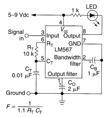
This circuit detects the presence of a 15-kHz audio signal and light the LED when it does so. (View)
View full Circuit Diagram | Comments | Reading(735)
SINGLE_COMPARATOR_WINDOW_DETECTOR
Published:2009/6/18 3:54:00 Author:May
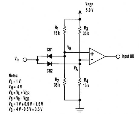
Simply by adding two steering diodes, a window detector can be built using only a single com-parator. The detector performs well for windows of about 1 V or greater, but it isn't suitable where extreme precision is required because the forward drops of the diodes vary.In the basic circuit, two resistive dividers set threshold voltage levels at both the inverting and noninverting inputs of the comparator by dividing the reference voltage. The input voltage is steered to the appropriate comparator input by diodes CR1 and CR2.When the input voltage is within the window, neither diode conducts, and the comparator is bi-ased for a high output. When the input goes above the window, CR2 conducts and pulls the inverting input high, causing the comparator output to go low. When the input voltage goes below the window, CR1 conducts, pulling the noninverting input low, again causing the comparator output to go low. The source resistance of Vinmust be low compared to the equivalent parallel resistance of each divider. (View)
View full Circuit Diagram | Comments | Reading(1623)
LM556_FREQUENCY_DETECTOR
Published:2009/6/18 3:51:00 Author:May
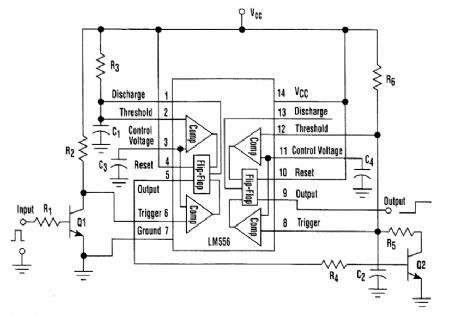
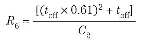
The circuit (see the ftgure), is built around an LM556 dual-timer IC. The 556's first timer is wired as a one-shot and is used to stretch the incoming pulses into fixed-length pulses. The second timer, which is similar to an astable multivibrator (pin 13 remains disconnected), functions as follows:The one-shot's fixed-length pulses, which are output on pin 5, turn on Q1 and discharge C2 through R5. If the frequency of the pulses is high enough, the voltage on C2 will fall below1/3 VCC and the second timer's output, pin 9, will go to a logic 1. Conversely, if the frequency is low enough or is zero, the voltage on C2 will charge through R6 to a level above2/3 VCC, and the pin 9 output will go to a logic 0. The idea is to keep the upper and lower peak voltage on C2 below 2/3 VCC and1/3 VCC, respectively for a logic 1, and above2/3 VCC and1/3 VCC, respectively, for a logic 0.To find the one-shot values, R3 and C1, select a pulse width (1.1 × R3 × C1) that's greater than the largest input pulse width and less than twice the inverse of the highest input frequency. To find R5, R6, and C2, first determine the duty cycle (ton/toff) of the input signal. Next, choose a standard value for C2 and calculate R6:Also, R5 = R6 (ton/toff). A tweak of resistors R5 and R6 might be needed to get the preferred response. Input signals with low duty cycles work the best. Finally, notice that capacitors C3 and C4 can be any value between 0.01 and 0.1 μF. (View)
View full Circuit Diagram | Comments | Reading(3041)
EXTENDED_ON_TIME_TIMER
Published:2009/6/18 3:45:00 Author:May


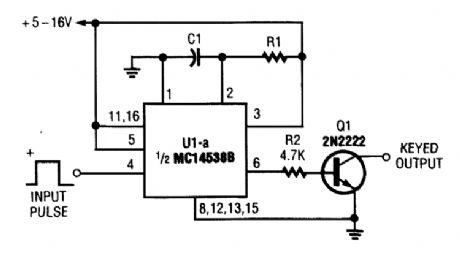

Half of a Motorola MC14538B dual, precision, retriggerable monostable multivibrator is used to form an extended on-time timer circuit. That type of circuit can be used as a switch debouncer. Such circuits are often used in digital circuitry, where each and every bounce of a switch contact is seen as a separate digital input.The delay on tirne (established by C1 and R1) is easily set using the formula, C1xR1, =T, where C1 is in microfarads,R1, is in megohms, and T is in seconds. (View)
View full Circuit Diagram | Comments | Reading(2980)
POPULAR_ELECTRONICS
Published:2009/6/18 3:42:00 Author:May
View full Circuit Diagram | Comments | Reading(1106)
DOUBLE_ENDED_LIMIT_DETECTOR
Published:2009/6/18 3:42:00 Author:May
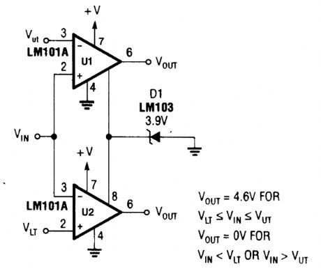
View full Circuit Diagram | Comments | Reading(0)
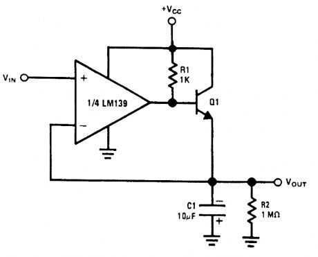
NEGATIVE_PEAK_DETECTOR
Published:2009/6/18 3:41:00 Author:May
View full Circuit Diagram | Comments | Reading(0)
GRID_LEAK_DETECTOR
Published:2009/6/18 3:41:00 Author:May
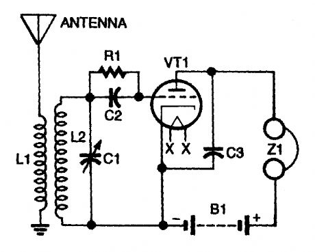
Tuned-cirfuit receiver with grid-leak detection. (View)
View full Circuit Diagram | Comments | Reading(983)
COUNT_DOWN_TIMER
Published:2009/6/18 3:41:00 Author:May
With switch S1 in the off position, as shown, battery voltage is applied across timing-capacitor C1, which stays chargedwhile the rest of the circuitryhas no power supplied to it. Transistor Q1, and thus transistors Q2 through Q4, are kept in an off condition as long as C1 has a sufficient charge. (View)
View full Circuit Diagram | Comments | Reading(806)
MOBILE_RADIO_ON_ALARM_TIMER
Published:2009/6/18 3:33:00 Author:May

This system will prevent you from accidentally leaving your mobile radio on, draining the battery.LED1 will light when the vehicle's ignition is on, or while the car is running. Switch S1 in the ON po-sition will close relay K1, completing the power circuit to the equipment. If the ignition switch is shut off, and switch S1 is still in the ON position, an alarm (piezo) will begin to beep and LED2 will flash.Returning S1 to the center position will shut everything off. If equipment operation is desired after shutting off the vehicle, you can place switch S1 in the AUT0 position and momentarily press S2, a normally open push-button switch. Depressing this switch begins a timing cycle. The length of time that the Mobile-ON alarm/timer operates before shutting everything off can be prograrrtmed by se-lecting R6. The approximate time delays are provided in the chart with the schematic. Or, you could change the value of C6. These components control the holding time of relay K1. LED3 will light while the circuit is in AUT0 status. Incidentally, you can also cartcel the time delay at any time during the delay period by simply switching it off. (View)
View full Circuit Diagram | Comments | Reading(721)
GLITCH_DETECTOR
Published:2009/6/18 3:33:00 Author:May
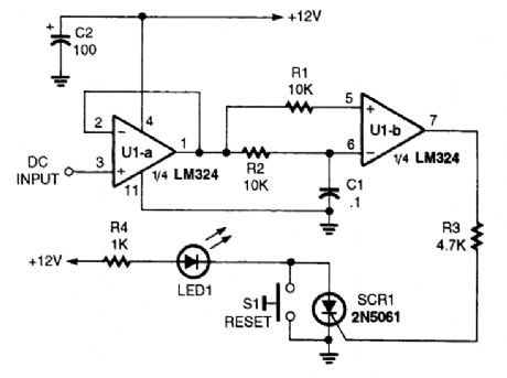
In the circuit, two op amps (half of an LM324 quad op amp) and an SCR are direct coupled in a dc-voltage monitoring circuit. Op-amp UI-a is configured as a voltage follower, which feeds the bridged in-puts of the second op amp, U1-b. A resistor/capacitor combination (R2/C1) connected to the negative input of U1-b forms an RC time-delay circuit. As long as there is no change in the dc-voltage level at either of UI-b's inputs, its output is near zero. If a voltage glitch occurs, the RC timing circuit will delay the voltage change at the op amp's inverting input, causing its output to go high, triggering SCR1 and causing LED1 to light. The circuit's sensitivity allows it to detect voltage changes in the millivolt range.Pressing S1 diverts the SCR's holding current to ground, causing it to turn off and reset the circuit. (View)
View full Circuit Diagram | Comments | Reading(2117)
WIDE_RANGE_TIMER_lMINUTE_TO_400_HRS
Published:2009/6/18 3:33:00 Author:May
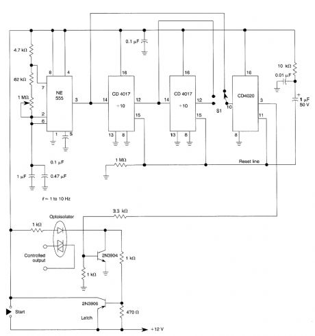
This ultra wide range timer uses a 555 timer base, two 4017Bs and a 4020B that act as frequency dividers that can be switched in and out. S1 is a SP3T range switch. (View)
View full Circuit Diagram | Comments | Reading(995)
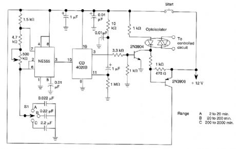
LONG_PERIOD_TIMER
Published:2009/6/18 3:21:00 Author:May
By using a 555 timer, time intervals of 150 minutes 60 hours can be generated with this circuit. (View)
View full Circuit Diagram | Comments | Reading(2)
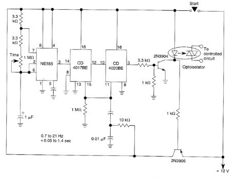
2_TO_2000_MINUTE_TIMER
Published:2009/6/18 3:20:00 Author:May
A CD4020B divider is used to divide the frequency of a 555 timer.S1 is a range selector switch that provides timing intervals of 2-20,20-200 and 200-2,000 minutes. (View)
View full Circuit Diagram | Comments | Reading(853)
LINEARIZED_RF_DETECTOR
Published:2009/6/18 3:16:00 Author:May
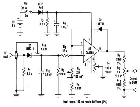
The circuit produces an extremely linear dc output for RF inputs between 80 mV rms and 4.0 mV rms. For inputs below 50 V rms, the dc output quickly drops to 0 V. (View)
View full Circuit Diagram | Comments | Reading(945)
LOCK_DETECTOR
Published:2009/6/18 3:11:00 Author:May
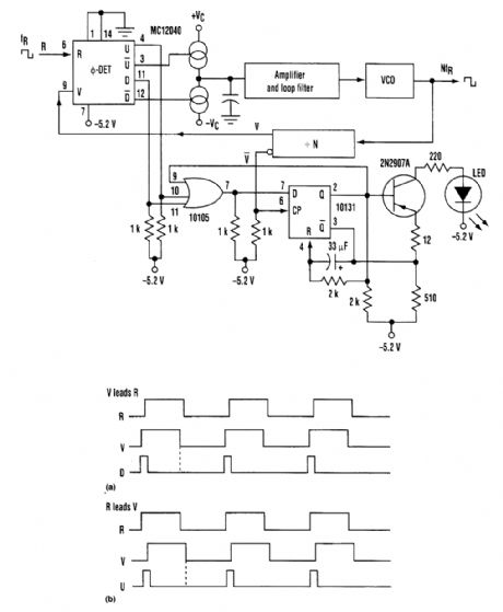
This PLL lock indicator not only can detect a 'locked or off-of-lock condition, but also even if a single pulse or transition has been missed.When being sampled by the flip-flop, if the V signal leads the input reference signal R and the rising edge of /i is lost, the D signal will remain hign throughout the interval, allowing the flip-flop to be clocked high (Fig. 26-2A). If the R signal leads the V signal when the transition is missed, the rising edge of the Tsignal will trigger the D signal of the phase detector, causing the LED to blink (Fig. 26-2B).A lock detector often is used with a phase-locked loop (PLL) or synthesizer to indicate when the loop is phase-locked with an input signal. This circuit can be helpful, but single cycle skips usu-ally frill go undetected because of the presence of the low-pass filter. (View)
View full Circuit Diagram | Comments | Reading(2307)
HIGH_SPEED_PEAK_DETECTOR_WITH_HOLD_AND_RESET_CONTROLS
Published:2009/6/18 3:08:00 Author:May
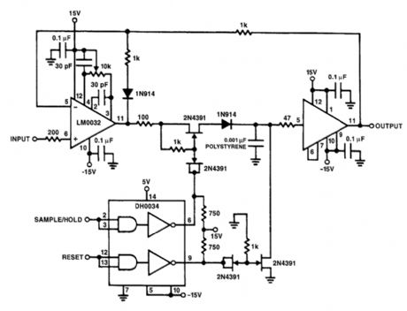
The LH0033 and LH0063 are useful in high-speed sample-and-hold or peak detector circuits be-cause of their very high speed and low-bias-current FET input stages. The high-speed peak detector circuit shown could be changed to a sample-and-hold circuit simply by removing the detector diode and reset circuitry. For best accuracy, the circuit can be trimmed with the 10-kΩ offset adjustment pot shown. The circuit has a typical acquisition time of 900 ns, to 0.1% of the final value for the 10-V input step signal, and a droop rate of 100 μV/ms, Even faster acquisition time can be achieved by re-ducing the hold capacitor value. (View)
View full Circuit Diagram | Comments | Reading(5282)
VIDEO_LINE_DECODER_II
Published:2009/6/18 2:57:00 Author:May
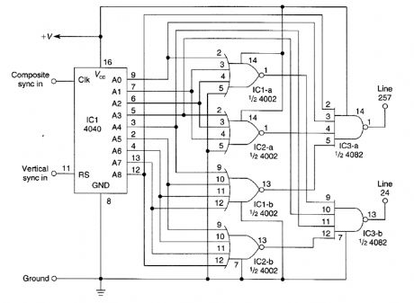
pulses useful for gating lines 24 and 257 of a video signal, but by chang-lines can be decoded. (View)
View full Circuit Diagram | Comments | Reading(700)
VIDEO_LINE_DECODER_I
Published:2009/6/18 2:55:00 Author:May
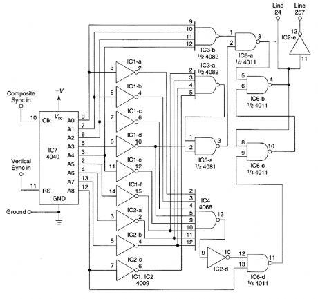
This line decoder uses only one pin for the line indicator. (View)
View full Circuit Diagram | Comments | Reading(865)
| Pages:81/101 At 2081828384858687888990919293949596979899100Under 20 |
Circuit Categories
power supply circuit
Amplifier Circuit
Basic Circuit
LED and Light Circuit
Sensor Circuit
Signal Processing
Electrical Equipment Circuit
Control Circuit
Remote Control Circuit
A/D-D/A Converter Circuit
Audio Circuit
Measuring and Test Circuit
Communication Circuit
Computer-Related Circuit
555 Circuit
Automotive Circuit
Repairing Circuit