
Measuring and Test Circuit
Index 92
The outline circuit of the pillar electric approaching sensor (2)
Published:2011/6/11 21:05:00 Author:qqtang | Keyword: outline circuit, pillar electric approaching sensor
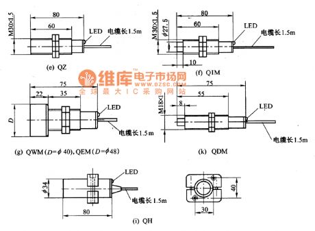
figure:The outline the pillar electric approaching sensor (2) (View)
View full Circuit Diagram | Comments | Reading(598)
The outline circuit of the pillar electric approaching sensor
Published:2011/6/11 21:04:00 Author:qqtang | Keyword: outline circuit, pillar electric approaching sensor
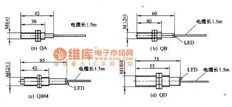
Figure: the outline of the pillar electric approaching sensor (View)
View full Circuit Diagram | Comments | Reading(549)
The frequency shift demodulator circuit composed of active filter
Published:2011/6/16 21:09:00 Author:qqtang | Keyword: frequency shift demodulator, active filter
Replacing LC modulation circuit by the active filter, we can avoid using large and expensive inductance coils in frequency shift key control demodulator, it is not only small in size, but also improves the function of the demodulator. This circuit is used to demodulate the 100 byte frequency shift key control signal, whose symbol frequency is 2225Hz, open frequency is 2025Hz. The filter A allows the open frequency to pass, and the filter B allows the symbol frequency to pass, therefore , when the symbol frequency in on the input terminal, the transistor is saturated and the output is short.
(View)
View full Circuit Diagram | Comments | Reading(1998)
The TDA5101A ASK 315 MHz emitter circuit
Published:2011/6/16 20:26:00 Author:qqtang | Keyword: emitter circuit
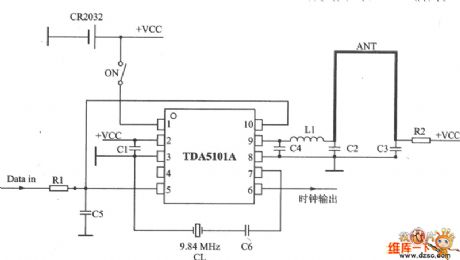
TDA5101A is an emitter chip with high-power amplifiers, which can be used in the non-key input system, remote control system, communication system and secure system. Its technological features are as follows: the working frequency is 315 MHz; ASK modulation method; the voltage of the power supply is 2.1v~4v; it has low-voltage detection output; the maximum working current is 9mA(emitting function), the standby current is 100nA; it has a efficient power amplifier. The circuit can drive a loop aerial and the current is low, which prolongs the life span of the battery.
(View)
View full Circuit Diagram | Comments | Reading(933)
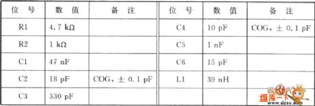
The digital frequency shift demodulator circuit (CA3020, MC723 and MC724)
Published:2011/6/16 21:39:00 Author:qqtang | Keyword: frequency shift demodulator
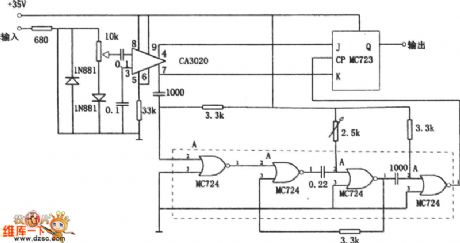
In the figure is the digital frequency shift demodulator circuit. This circuit can be used in frequencies from 1kHz to 10kHz, and it can demodulate the frequency drifting of 1%. The input stage of the circuit consists of the wide band amplifier CA3020, whose differential output is added on the input terminal of J-K trigger. The gate circuit MC724 forms a single stable multi-resonance oscillator. The timing period of the oscillator is equal to the half period of the central frequency. The input signal passes the trigger after being lagged by the oscillator. For example, the 2920Hz means the symbol, the 2750Hz means blank space.
(View)
View full Circuit Diagram | Comments | Reading(687)
The DTMF wireless calling system circuit
Published:2011/6/21 1:49:00 Author:Seven | Keyword: wireless calling system

By the dual sound multi-frequency encoding signal, the circuit modulates the emitted carrier frequency, and it composes a DTMF encoding wireless calling system circuit. The circuit uses DTMF encoding circuit UM97085 and decoding circuit YN9101 to form a micro wireless calling system, which is used in small enterprises, and it is convenient and economic. See as the figure, (a) represents the DTMF encoding wireless electric emitting circuit, (b) represents the wireless electric reception demodulating, DTMF decoding and stereo signal sound system.
(View)
View full Circuit Diagram | Comments | Reading(2261)
Precise light diode comparator circuit
Published:2011/6/22 3:26:00 Author:TaoXi | Keyword: Precise, light diode, comparator
The R1 sets the comparison level. When it is comparing, the voltage drop of the light diode is lower than 5mV, the dark current reduces a magnitude. The integrated circuit is LM111/211/311.
(View)
View full Circuit Diagram | Comments | Reading(645)
Shaft rotation status detection circuit
Published:2011/6/22 19:24:00 Author:TaoXi | Keyword: Shaft, rotation, status, detection circuit
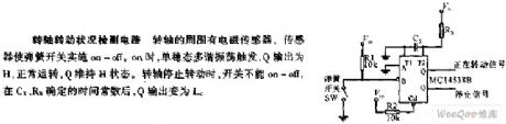
The shaft rotation status detection circuit: there are some electromagnetic sensors around the shaft, these sensors make the spring switch to turn on and off. When the switch is at the on position, the monostable multivibrator is triggered, the Q outputs the H, the operating is normal, Q maintains the H state. When the shaft stops turning, the switch can not turns on and off, after the Cx and Rx confirm the time constant, the output of Q is L.
(View)
View full Circuit Diagram | Comments | Reading(635)
The PLL FM demodulator (LM565CN、RC4558DN) circuit
Published:2011/6/16 20:48:00 Author:qqtang | Keyword: FM demodulator
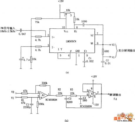
In the figure is a 10kHz±3kHz FM demodulator circuit consisting of LM565CN. The differential demodulation of V1 and V2 is level-shifted and amplified by A1 difference amplifier in figure (b), then the 20KHz pulse impulse momentum is removed by LPF composed of A2.
(View)
View full Circuit Diagram | Comments | Reading(2835)
The bilateral band modem circuit composed of NE561B
Published:2011/6/16 20:55:00 Author:qqtang | Keyword: bilateral band, modem circuit
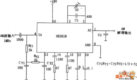
In the figure is the bilateral band modem circuit composed of NE561B. The loading frequency of the input modulating signal is f0=1MHz. When the AM modulation signal is added on the input terminal of the multiplier, it is also added on the phase detection circuit by Rv1, CY1, Y2 and CY2, and it sets the VCO frequency of PLL at f0.
(View)
View full Circuit Diagram | Comments | Reading(1826)
The moving object detector circuit
Published:2011/6/20 22:11:00 Author:Seven | Keyword: moving object, detector
The moving object detector circuit is shown in the figure:The above figure is the ultrasonic wave reception and process circuit, and its emitting circuit is this.
(View)
View full Circuit Diagram | Comments | Reading(1747)
The wide band linear detection circuit of 10MHz
Published:2011/6/16 20:13:00 Author:qqtang | Keyword: wide band, linear detection circuit
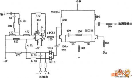
In the figure is the wide band linear detection circuit of 10MHz, which is used in measuring instruments like millivoltmeters. The computing amplifier is fixed with a wide band μPC53, whose output is amplified by the differential amplifier composed of the triode 2SC384. The diode in the circuit is Ge diode, by installing it in the backward feedback circuit, the power supply voltage is increased by the differential circuit.
(View)
View full Circuit Diagram | Comments | Reading(704)
Game-scoring Display Screen Circuit Diagram
Published:2011/6/16 10:58:00 Author:Vicky | Keyword: Game-scoring Display Screen
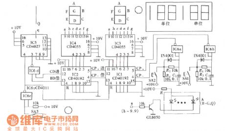
Game-scoring display screen circuit diagram is shown as in the above picture. The circuit is composed of add/subtract scoring input circuit, add/subtract scoring circuit, counting - decoding display circuit and reset circuit. (View)
View full Circuit Diagram | Comments | Reading(2092)
Unijunction Transistor (UJT) Work Performance Quick Test Circuit Diagram
Published:2011/6/18 10:21:00 Author:Vicky | Keyword: Unijunction Transistor (UJT) Performance Quick Test

The above picture is a circuit of unijunction transistor (UJT) work performance quick test .The tested unijunction transistor (UJT) VBT (suppose: BT33) constitutes relaxation oscillator together with R3 and C2. When the VBT is on, triode VT1 acquires bias current via bias resistance R2 (S1 is broke and S2 is closed up in the moment), and the luminous diode H1 gives out light. +10V power supply charges C2 via VD2 by R3. Voltmeter V can detect that the voltage of two ends of C2 would goes up continuously. When the electric potential of E end reaches the peak voltage, part from E to B1 of VBT would automatically breakover and the voltage of capacitance C1 would discharge via part from E to B1, both of which leads to emitter junction of triode VT1 ends because of back bias. (View)
View full Circuit Diagram | Comments | Reading(2018)
Quartz Crystal Selection Circuit Diagram
Published:2011/6/18 10:18:00 Author:Vicky | Keyword: Quartz Crystal Selection
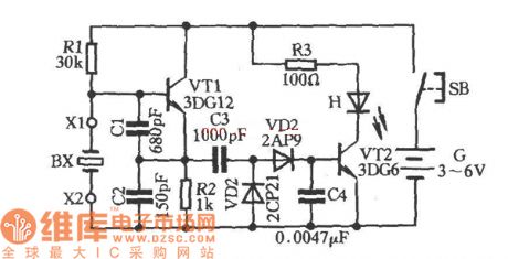
As shown in the above picture, BX is a Quartz Crystal (also called crystal oscillator) under test. Plug it into sockets X1 and X2, and press button SB. If BX is good, the oscillator composed of triode VT1, capacitances C1 and C2 works. The oscillator signal was sent from VT1 emitter, and coupled to VD2 via C3 to process detection and C4 filtering. It then becomes direct current and is sent to VT2 base electrode to make VT2 conducted and luminous diode H give out light, which is an indication that the quartz crystal is good. If H doesn’t give out light, then the quartz crystal is bad. By changing the capacitance value of C1 and C2 appropriately, it can be used to test quartz crystals of different frequency. (View)
View full Circuit Diagram | Comments | Reading(836)
The Otis toec-chvf elevator overhaul circuit
Published:2011/6/20 22:14:00 Author:Seven | Keyword: Otis, overhaul
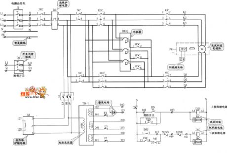
The Otis toec-chvf elevator overhaul circuit is shown as above. (View)
View full Circuit Diagram | Comments | Reading(2895)
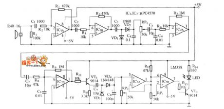
The instrument and meter circuit of the LED detector
Published:2011/6/19 22:04:00 Author:qqtang | Keyword: instrument, LED detector
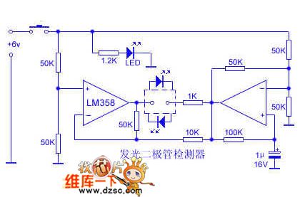
The LM358 tester can detect LED without polarity differentiating, so it can judge the lighting character of the LED. In the mass test, compared with the multimeter, it's time-saving and simple. See as the figure, a line of computing amplifier forms the low-frequency self-motivated oscillator, which outputs intermittent high LEV or low LEV on the output terminal. Another line of op-amp forms a phase inverter. When the oscillating circuit outputs high LEV, the inverter is outputting the low LEV; when the oscillating circuit outputs the low LEV, the inverter is outputting the high LEV.
(View)
View full Circuit Diagram | Comments | Reading(1416)
The sensitive frequency demodulator (LM565 and LM111) circuit
Published:2011/6/16 21:21:00 Author:qqtang | Keyword: sensitive frequency demodulator
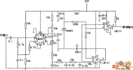
This circuit consists of the phase-lock integrated circuit LM565, which can track the frequency shift in a wide frequency range. However, to the low frequency signal, as the demodulating output signal is weak, the drifting of the voltage control oscillator will cause the drifting of the comparator working point and then cause faults. To overcome the above weakness, we add a DC recover part in the circuit, so it can work stably even when the frequency of the signal is weak. In the figure, the demodulating circuit composed of LM565 and comparator LM111 is almost the same with ordinary frequency demodulator circuits.
(View)
View full Circuit Diagram | Comments | Reading(1347)
The PLL FM demodulator (4046) circuit
Published:2011/6/16 21:26:00 Author:qqtang | Keyword: FM demodulator
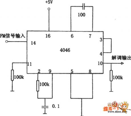
See as the figure, the FM demodulator (4046) circuit consists of 4046 PLL particles, the intermediate FM input signal is demodulated into the low frequency by the circuit.
(View)
View full Circuit Diagram | Comments | Reading(7526)
The 567 FM demodulator circuit
Published:2011/6/16 21:58:00 Author:qqtang | Keyword: FM demodulator circuit

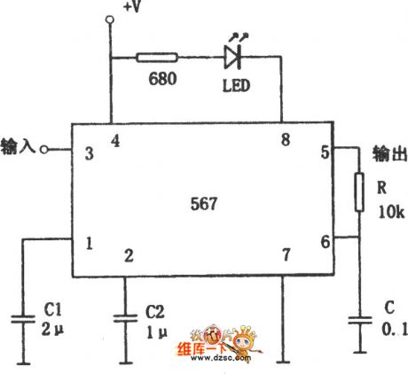
In the figure is the 567 FM demodulator circuit. In the figure, the FM signal is input from 3-pin and the demodulated signal is output from 5-pin. The central frequency of the FM signal that the circuit can demodulate is: fo=1.1/RC. In the circuit, C1 is the filtering capacitor, C2 is the wide band adjusting capacitor, when C2 is going down, the band width of the demodulator is rising. The selecting basis of C2 is:
There is also a demodulation indicating circuit. When the demodulation is right, 8-pin is outputting a low LEV. When the indicator is on, it is glowing, the indicator can also be pick out and used as the control signal.
(View)
View full Circuit Diagram | Comments | Reading(2640)
| Pages:92/101 At 2081828384858687888990919293949596979899100Under 20 |
Circuit Categories
power supply circuit
Amplifier Circuit
Basic Circuit
LED and Light Circuit
Sensor Circuit
Signal Processing
Electrical Equipment Circuit
Control Circuit
Remote Control Circuit
A/D-D/A Converter Circuit
Audio Circuit
Measuring and Test Circuit
Communication Circuit
Computer-Related Circuit
555 Circuit
Automotive Circuit
Repairing Circuit