
Measuring and Test Circuit
Index 85
0_2_A_BATTERY_CURRENT_MONITOR_WITH_DIGITAL_OUTPUT
Published:2009/6/17 1:49:00 Author:May
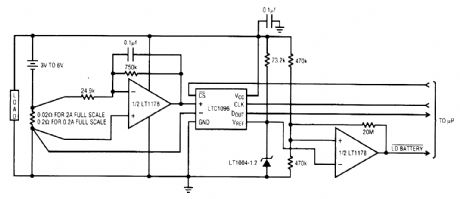
IC devices by Linear Technology make up this current monitor circuit 3- to 6-V battery. (View)
View full Circuit Diagram | Comments | Reading(735)
BATTERY_VOLTAGE_MONITOR
Published:2009/6/17 1:45:00 Author:May
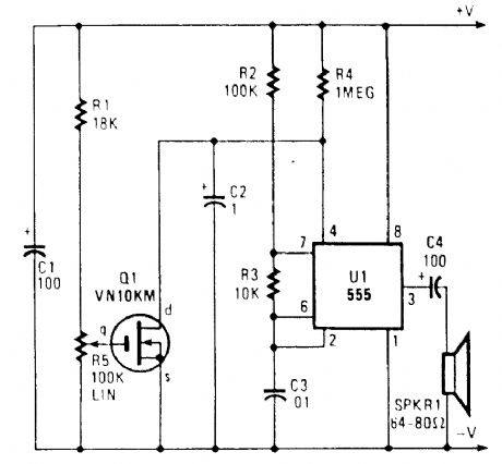
When battery voltage goes low, pin 4 of U1 goes high as Q1 fails to conduct. This activates oscillator U1 and generates audio tone. R5 sets level at which the circuit activates. (View)
View full Circuit Diagram | Comments | Reading(1013)
BATTERY_TEST_CIRCUIT
Published:2009/6/17 1:44:00 Author:May
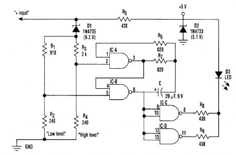
Using this circuit, three levels of voltage can be displayed-normal (11 to 15 V), high (>15 V), and low (<11 V). When the voltage is low, the LED glows steadily. In the normal range, the LED is off. When the voltage is high, the LED blinks at a 1-Hz rate. This circuit is useful for assuring proper electrical system operation. (View)
View full Circuit Diagram | Comments | Reading(750)
SIMPLE_LIE_DETECTOR
Published:2009/6/16 23:46:00 Author:May
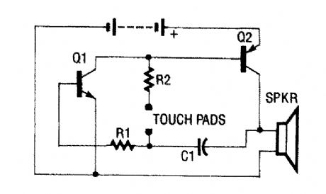
The circuit uses a two-transistor direct-coupled oscillator that has a frequency determined by C1, R2, and the (skin) resistance across the touch pads. Since C1 and R2 are fixed values, only the skin resistance across the touch pads can vary the sound of the oscillator. To sustain oscillations, C1 feeds a portion of the output from Q2 back to the input of Q1 through resistor R1.Transistor Ql is an npn type and transistor Q2 is a pnp type. The output of Q2 is fed into a small speaker. The circuit relies on the fact that the human skin conducts electricity.
C1 0.01-μF CapacitorQ1 2N3904 TransistorQ2 2N3906 TransistorR1 4.7kΩ ResistorR2 85kΩ Resistor (View)
View full Circuit Diagram | Comments | Reading(3002)
REMOTE_CONTROL_TESTER
Published:2009/6/16 22:28:00 Author:May
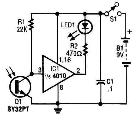
The IR Tester circuit lets you know if the but-ton you press on a remote control is working. Q1 is a photo transistor that is activated by IR energy. (View)
View full Circuit Diagram | Comments | Reading(1462)
SIMPLE_IR_DETECTOR
Published:2009/6/16 22:12:00 Author:May
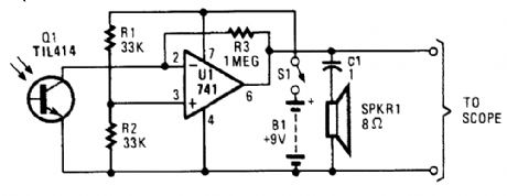
Useful for IR detection, this circuit uses an op amp of the 741 family (or similar) to detect and amplify IR pulses. (View)
View full Circuit Diagram | Comments | Reading(1536)
CAR_BATTERY_TESTER_FOR_CRANKING_AMPS
Published:2009/6/16 4:39:00 Author:May
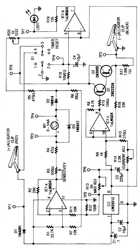
This circuit determines the cold cranking amps of a battery by firest discharging the surface charge, then checking the internal resistance. This gives a more realistic measurement than simply measuring the instantaneous drop in voltage with a load. A constant-current source draws 2.5A. Then, after one minute, a voltage drop measurement is made under load. (View)
View full Circuit Diagram | Comments | Reading(1057)
BATTERY_TESTER_
Published:2009/6/16 4:04:00 Author:May
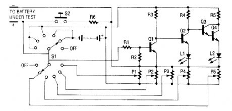
The battery tester uses four transistors and two LEDs to indicate the condition of any battery you want to test. Q3 and Q4 are connected in a Darlington configuration that has extremely high gain. LED L2 lights when a small positive potential appears on the base of Q3. Transistors Q1 and Q2 form a direct-coupled dc-amplifier circuit. The output of this stage drives the red LED L1. Rotary switch 51 is used to select different ranges (which have been previously set by adjusting trimmer resistors PI through P5).The positive (+) lead goes through the selected contacts of S1 to the biasing resistors R3, R4, and R5. The negative (-) lead of the battery under test goes to the ground or common lead of the circuit and the (+) side to one side of P1 through P5.L1 Red LEDL2 Green LEDP1 through P5 5-kΩ trimmer resistorR1 100 kΩR2, R3 33 kΩR4, R5 470 ΩR6 12 Ω 1WS1 2 P6 position NS rotary switchS2, NO pushbutton switchDepending on the position of S1, a particular trimmer resistor (wiper lead) is selected. That lead goes through the contact on S1 to resistor R1 and into the base of npn transistor Q1. If the battery is good enough, (+) voltage goes to the base of Q1, turning it on. This turns Q2 off, which then allows Q3 to turn on. That causes Q4 to turn on and light green LED L2.If the battery is weak, Q1 will not turn on, which will cause Q2 to be biased on by R3, which in turn lights red LED L1. When Q1 is on, it biases the base of Q3 negative, and causes Q3 to be turned off. That prevents L2 from turning on.The circuit operates in the same manner for all ranges except the first two, where a 9-V battery has been added by S1 to be in series with the input voltage to allow for testing of very low voltage batteries. That is because at voltages below 2 Vdc, LEDs will not light and the circuit would be unable to set a low-voltage (<2-V) battery without the additional internal-battery voltage. A load resis-tor has also been included; it allows the battery under test to be connected to a load to give a better indication of its condition. That load resistor is connected across the battery when normally open (NO) switch S2 is depressed. (View)
View full Circuit Diagram | Comments | Reading(959)
AUTO_FUSE_MONITOR
Published:2009/6/16 3:00:00 Author:May
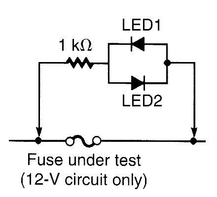
This circuit can quickly check a fuse in an automobile circuit. Connect across suspected fuse-either LED glows, fuse is blown. The circuit must be live for this test to work. (View)
View full Circuit Diagram | Comments | Reading(853)
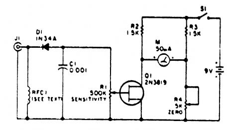
SIMPLE_FIELD_STRENGTH_METER_Ⅱ
Published:2009/6/16 2:16:00 Author:May
This simple field-strength meter provides a cheap way to monitor an amateur radio or CB transmitter (or even an antenna system) for maximum output. (View)
View full Circuit Diagram | Comments | Reading(1388)
SIMPLE_FIELD_STRENGTH_METER_I
Published:2009/6/16 2:15:00 Author:May
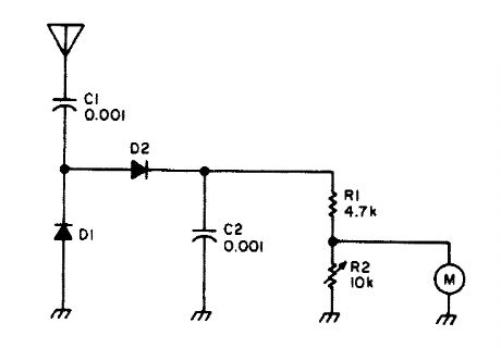
Useful for checking transmitters and anten-nas, this circuit uses a voltage-doubling detector D1 and D2 (HP 5082-2800 hot carrier types). D1 and D2 can also be type IN34 or IN82. M is a 100-mA meter movement. (View)
View full Circuit Diagram | Comments | Reading(677)
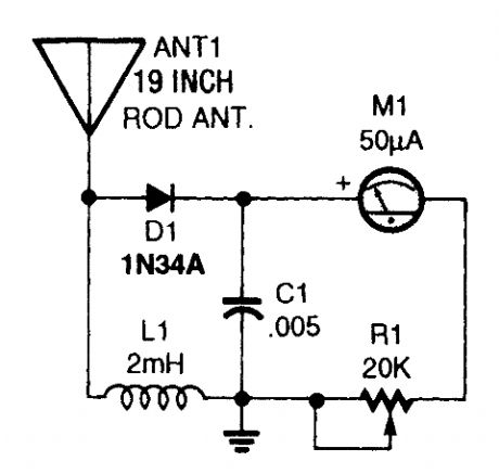
SIMPLE_AMPLIFIED_FIELD_STRENGTH_METER
Published:2009/6/16 2:14:00 Author:May


This circuit uses a FET as a dc amplifier in a bridge circuit. R4 is set for meter null with J1 short circuited. Any surplus 50-mA meter can serve in this circuit. RFC1 is any suitable RE choke for the band in use. A 2.5-mH RE choke will do for broadband operation. R1 is a sensitivIty control. The antenna can be any small whip antenna (2 ft or less). (View)
View full Circuit Diagram | Comments | Reading(1087)
LOW_DRIFT_PEAK_DETECTOR
Published:2009/6/15 22:55:00 Author:May
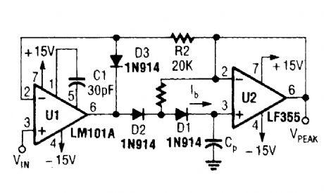
Leakage of D2 is provided by feedback path throtlgh Rf Leakage of circuit is essenttany lb(LF155,LF156) plus capacitor leakage of Cp Diode D3 clamps Vout (Al) to Vin-VD3 to improve speed and to limit reverse bias of D2 Maximum input frequency should be<<1/2πRfCD2,where CD2 is shunt capacitance of D2 (View)
View full Circuit Diagram | Comments | Reading(3022)
NEGATIVE_PEAK_DETECTOR
Published:2009/6/15 22:39:00 Author:May
View full Circuit Diagram | Comments | Reading(1)
AIR_FLOW_DETECTOR
Published:2009/6/15 22:39:00 Author:May
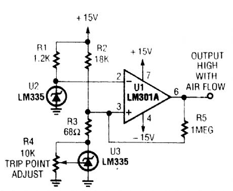
Two precision temperature sensors are used to detect a small temperature difference. When air flow occurs, self-heating of the LM335 is re-duced, and the output of the two temperature sensors is unequal. This is amplified by U1. (View)
View full Circuit Diagram | Comments | Reading(3348)
FAST_PULSE_DETECTOR
Published:2009/6/15 22:37:00 Author:May
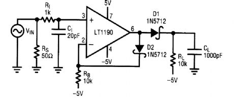
A fast pulse detector can be made with this circuit. A very fast input pulse will exceed the am-plifier slew rate and cause a long overload recovery time. Some amount of dv/dt limiting on the input can help this overload condition, however this will delay the response. (View)
View full Circuit Diagram | Comments | Reading(886)
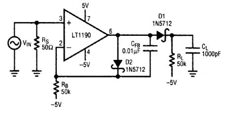
CLOSED_LOOP_PEAK_DETECTOR
Published:2009/6/15 22:33:00 Author:May
This closed-loop peak detector circuit uses a Schottky diode inside feedback loop to obtain good accuracy. The 20-Ω resistance R, isolates the 0.01-μF load and prevents oscillation. The dc value is read with a DVM. At a low frequency, the error is small and dominated by the decay of the detector capacitor between cycles. As the frequency rises, the error increases because capacitor charging time decreases. During this time, the overdrive becomes a very small portion of a sine-wave cycle. Finally, at approximately 4 MHz, the error rises rapidly because of the slew-rate lim-itation of the op amp. (View)
View full Circuit Diagram | Comments | Reading(2508)
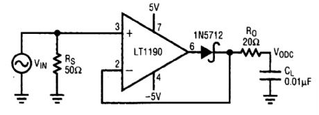
OPEN_LOOP_PEAK_DETECTOR
Published:2009/6/15 22:33:00 Author:May
In this open-loop design, the detector diode is D1, and a level shifting or compensating diode is D2. Load reststor RL is connected to -5V, and an identical bias resistor RL is connected to -5 V, and identical bias resistor RL is used to bias the compensating diode. Resistors with equal values ensure that the diode drops are equal. Low values of RL and RB (1kΩ to 10kΩ) provide fast response, but at the expense of poor low-frequency accuracy. High values of RL and RB provide good low-frequency accuracy, but cause the amplifier to slew rate limit, resulting in poor high-frequency accuracy. A good compromise can be made by adding a feedback capacitor CFB which enhances the negative slew rate on the (-) input. (View)
View full Circuit Diagram | Comments | Reading(758)
SIMPLE_FULL_WAVE_ENVELOPE_DETECTOR
Published:2009/6/15 22:26:00 Author:May
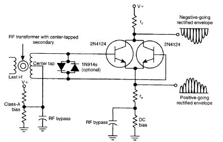
Simple, yet sensitive, this amplifying full-wave detector circuit has an almost zero rectification threshold. It presents a highly linear RF load to the final IF stage. The gain for the collector output is given (approximately) by rc/re, The emitter output gain is slightly less than unity. (View)
View full Circuit Diagram | Comments | Reading(1105)
BUG_DETECTOR
Published:2009/6/15 22:16:00 Author:May
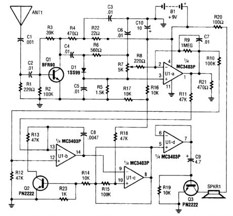


The circuit, built around a single integrated circuit (U1, an MC3403P quad op amp), three tran-sistors (Q1-Q3), and a few support components, receives its input from the antenna (ANTI). The signal is fed through a high-pass filter, formed by C1, C2, and RI, which eliminates bothersome 60-Hz pickup from any nearby power lines or line cords located in and around buildings and homes.From the high-pass filter, the signal is applied to transistor Q1 (which prov'tdes a 10-dB gain for frequencies in the 1- to 2000-MHz range) for amplification. Resistors R2, R3, and R4 form the biasing network for Q1. The amplified signal is then ac coupled, via capacitor C4 and resistor R7's (the sensi-tivity control) wiper, to the inverting input (pin 2) of U1-a. Op amp U1-a is configured as a very high gain amplifier. With no signal input from ANTI, the output of U1-a at pin 1 is near ground potential.When a signal from the antenna is applied to the base of Q1, it turns on, producing a negative-go-ing voltage at the cathode of Dl. That voltage is applied to pin 1 of UI-a, which amplifies and inverts the signal, producing a positive-going output at pin 1. Op amps UI-b and UI-c along with CS, RIO through R18, and Q2 are arranged to form a voltage-controlled oscillator fi/CO) that operates over the audio-frequency range. As the output of U1-a increases, the frequency of the VC0 increases. The VCO output, at pin 8 of U1-c, is fed to the input of U1-d, which is configured as a noninverting, unity-gain (buffer) amplifier. The output of U1-d is used to drive Q3, which, in turn, drives the output speaker. (View)
View full Circuit Diagram | Comments | Reading(3281)
| Pages:85/101 At 2081828384858687888990919293949596979899100Under 20 |
Circuit Categories
power supply circuit
Amplifier Circuit
Basic Circuit
LED and Light Circuit
Sensor Circuit
Signal Processing
Electrical Equipment Circuit
Control Circuit
Remote Control Circuit
A/D-D/A Converter Circuit
Audio Circuit
Measuring and Test Circuit
Communication Circuit
Computer-Related Circuit
555 Circuit
Automotive Circuit
Repairing Circuit