
Measuring and Test Circuit
Index 88
High precision pressure test system circuit composed of the MAX1463
Published:2011/7/8 5:08:00 Author:Christina | Keyword: High precision, pressure, test system
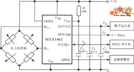
The high precision pressure test system circuit which is composed of the MAX1463 is as shown in the figure. The output voltage of the bridge type pressure sensor is connected with the IN1+ and IN1- ports of MAX1463. Under the control of CPU, the pressure signal is nonlinearly calibrated and temperature compensated and D/A converted by the circuit, then it is output by the serial interface to the 80C51 single-chip microcomputer; it also changes into the analog output voltage Uo and adds to the digital voltmeter to display the tested pressure value. The GPI01 pin of the general digital I/O interface is connected with the fault alarm, when the lead of the sensor is open-circuit or the CPU overflows, the buzzer will send out the sound of alarm.
(View)
View full Circuit Diagram | Comments | Reading(546)
Circuit Diagram of SL322-Type Flexible and Light-Spot Displaying Level Indicator
Published:2011/7/2 0:04:00 Author:Vicky | Keyword: Flexible and Light-Spot Displaying , Level Indicator
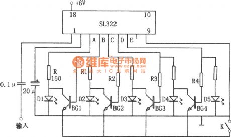
The circuit is made of luminous display driver SL322, luminous diodes from D1 to D5, transistor from BG1 to BG5 etc.
When K is closed, all the triodes’ emitters are in ground connection state. When the level rises to make luminous diode D2 give out light, electrical potential of B rises, BG1 is conducted, and then the luminous diode D3 goes out. When the electrical potential rises to make the D3 luminous, then electrical potential of C rises, BG2 is conducted, and thereby D2 goes out. In the context, due to the unchanged electrical potential of B, BG1 is still off, and D1 is still lightless. Ultimately, when the electrical potential rises to make D5 give out light, transistors form BG1 to BG4 are conducted, and luminous from D1 to D4 all die out, which formulates light-spot displaying. When the switch K is disconnected, all triodes stop working, and the light-spot displaying ends. (View)
View full Circuit Diagram | Comments | Reading(681)
Circuit Diagram of Audio Logic Level Probe Composed of 555
Published:2011/7/2 22:11:00 Author:Vicky | Keyword: Audio Logic Level Probe
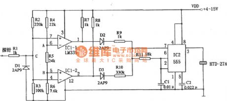
The above picture is audio logic level probe circuit, which is composed of voltage comparator, multivibrator, and piezoelectric ceramics HTD etc. The latter two constitute audio circuit and the audio frequency is used to assess the TTL or COMOS instrument’s electrical level.
When the probe reaches high level, IC-1 sends out signal to make D2 conducted and charge C1 via R9 and R11. The oscillator works, and the correspondent oscillating frequency is fH=1.44/(R10+2R11)C1, the correspondent frequency of the parameter in the picture is abouth 4kHz. When the probe reaches low level, the matched D3 is conducted, and C1 is charged via R10 and R11. The correspondent oscillator circuit works with oscillating frequency of fL=1.44/(R10+2R11)C, and the correspondent frequency of the parameter in the picture is about 700Hz. When pulse train is detected, the correspondent HTD sends out mixed sound or trill sound. (View)
View full Circuit Diagram | Comments | Reading(2124)
Simple-Adjustment Type High Input Impedance Double-Wave Linear Detection (CR4558DN) Circuit Diagram
Published:2011/7/1 23:57:00 Author:Vicky | Keyword: Simple-Adjustment, High Input Impedance Double-Wave Linear
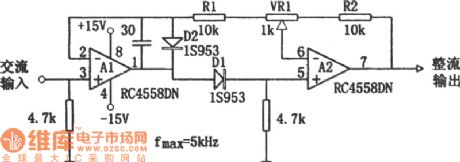
The above picture is a simple-adjustment type high input impedance double-wave linear detection circuit.
In the positive semi-circle of output AC signal, the output of A1 is positive, and forward biased D1 is conducted, and therefore both the input and output of A2 are positive. Use R2, VR1,and R1 to perform reverse feedback of β=1 towards A1, that is to say, to change A to be non-inverting amplifier with gain of 1 . Under such circumstance, the gain remains unchanged when modulate VR1.
In the positive semi-circle of the output signal, the output of A1 is negative, D1 is reverse biased, the output of A2 is 0, and therefore A2 becomes inverting amplifier. A1 conducts reverse feedback via D2. In fact, A1 becomes voltage follower. The reverse output of A2 is identical with AC input voltage, and A2 works as a invert amplifier with gain of 1. Under such circumstance, the gain of A2 can be changed by modulating VR1. Modulate VR1 to ensure that the whole gain is 1. (View)
View full Circuit Diagram | Comments | Reading(686)
Temperature measurement circuit composed of the AD7714 and Pt100
Published:2011/7/7 2:11:00 Author:Christina | Keyword: Temperature measurement
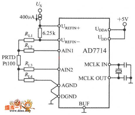
The temperature measurement circuit which is composed of the AD7714 and Pt100 is as shown in the figure. The Pt100 uses the 4-wire connection method, this method can eliminate the voltage drop of the lead resistances RL3 and RL2. The external 400μA current source supplies the PT100 excitation current, and this current produces the reference voltage of AD7714 through the 6.25kΩ resistance. Because the change of input voltage and the reference voltage is proportional to the change of the excitation current. so the change of excitation current will not affect the measurement precision. In order to avoid the influence of the temperature change, the 6.25kΩ resistance need to use the low temperature coefficient metal film resistance.
(View)
View full Circuit Diagram | Comments | Reading(13555)
Pressure measurement system composed of the AD7714
Published:2011/7/7 3:39:00 Author:Christina | Keyword: Pressure, measurement system
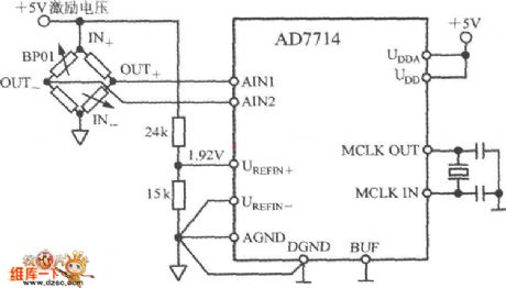
The pressure measurement system which is composed of the AD7714 is as shown in the figure. The BP01 is designed as the pressure sensor which is produced by the Sensym company. You need to connect the BP01 into the bridge circuit, the OUT+ and OUT- ports output the differential voltage. If you add the rated full scale pressure on the pressure sensor, the sensitivity of the differential output voltage is 3mV/V. If you use the +5V excitation voltage, the full-scale output range of the sensor is ±15mV. This excitation voltage is divided by the 24kΩ and 15kΩ resistances to supply the 1.92V benchmark voltage for the AD7714, so the fluctuation of the excitation voltage will not cause the measurement error.
(View)
View full Circuit Diagram | Comments | Reading(757)
Temperature measurement circuit composed of the AD7714 and the thermocouple
Published:2011/7/6 21:46:00 Author:Christina | Keyword: Temperature measurement, thermocouple
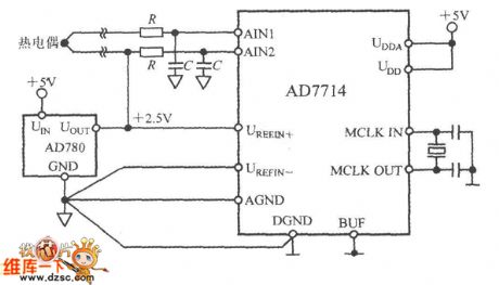
The temperature measurement circuit which is composed of the AD7714 and the thermocouple is as shown in the figure. In this application, the AD7714 operates in the buffer mode, this mode can connect with the decoupling capacitor at the front port to filter the noise on the thermocouple leads. In the buffer mode, the common mode range of AD7714 is narrow, in order to make the differential voltage of the thermocouple in the right common-mode voltage range, the AIN2 input port of the AD7714 should be offset to the +2.5V benchmark voltage.
(View)
View full Circuit Diagram | Comments | Reading(914)
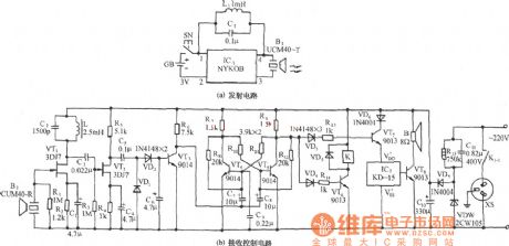
MK5087+TWH630 Remote control transmit circuit
Published:2011/7/4 0:29:00 Author:John | Keyword: Remote control
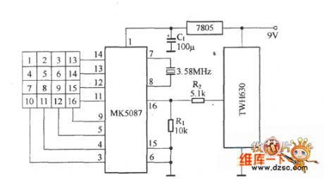
MK5087+TWH630 Remote control's transmit circuit is shown.
(View)
View full Circuit Diagram | Comments | Reading(1310)
Circuit Diagram of Gaining 0~284V Voltage by concatenation of 2 voltage regualtor
Published:2011/6/25 10:47:00 Author:Vicky | Keyword: 0~284V Voltage, concatenation of 2 voltage regualtor
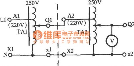
As shown in the picture, by concatenation of 2 voltage regulator, 0~284V voltage then is gained. Connect X1 and X2 of TA1 and TA2 respectively together by a conductor trace line, and then connect them to null line N of power supply; connect Al and X1 to power supply of 220V. Connect TA1 output end Q1 to end A2 of TA2. After energized, 0~ 284 voltage also can be gained in the TA2 output end Q2 and the voltage regulating is smooth. (View)
View full Circuit Diagram | Comments | Reading(608)
Tap Moving-Direction Display Circuit Diagram
Published:2011/6/27 18:54:00 Author:Vicky | Keyword: Tap Moving-Direction Display
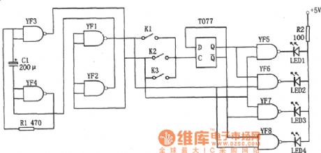
The above picture is a tap moving direction display circuit. The circuit is composed of micropulser, D trigger (T077), decoding circuit, and luminous diodes LED1~LED4 etc.
Micropulse iscomposed of 4 NAND gates from YF1 to YF4, with output signal frequency between 1 and 3 Hz. The frequency can be adjusted by changing the value of C1 and R1.Decoding circuit is composed of 4 NAND gates from YF5 to YF8. It’s output signal control the displaying of luminous diode, so that when the recorder works, light is given out from LED1 to LED4 in succession to indicate the direction the tape moves.
(View)
View full Circuit Diagram | Comments | Reading(650)
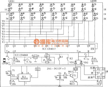
Circuit Diagram of Electronic Guidepost Composed of 555 and CD4017
Published:2011/7/4 10:07:00 Author:Vicky | Keyword: Electronic Guidepost
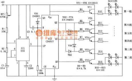
Electronic guidepost is shown as the picture. Its displaying circuit consists of 24 luminous diodes which are ranked in 6 groups in accordance with the direction of arrows. Electronic guidepost uses the pulse signal generated by time-base circuit to drive the 6 groups of luminous diodes to display dynamically according to a certain regular pattern so as to indicate the moving direction. The circuit is mainly composed of time-base circuit 555, decimal counter CD4017 and display circuit. (View)
View full Circuit Diagram | Comments | Reading(1125)
Circuit Diagram of Gaining 0~433V voltage by star connection of three voltage regulators
Published:2011/6/25 10:47:00 Author:Vicky | Keyword: 0~433V voltage, star connection of three voltage regulators
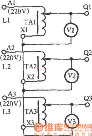
As shown in the picture, by adopting star connection of three voltage regulator (TA1, TA2, and TA3), the range of voltage regulating is expanded and the highest voltage can be 433V. Connect X1, X2 and X3 together which belong to TA1, TA2 and TA3 respectively, and connect A1, A2, and A3 triphase L1, L2 and L3 of 380V power supply, so that 433V voltage is gained in the output end of Q1 and Q2 or Q2 or Q3. However, this connection methond requires balance of triphase voltage, and the type and specification of TA1, TA2, and TA3 should also be the same. (View)
View full Circuit Diagram | Comments | Reading(710)
Voltage Regulator Voltage and Load Test Circuit Diagram
Published:2011/6/25 10:43:00 Author:Vicky | Keyword: Voltage Regulator Voltage and Load Test
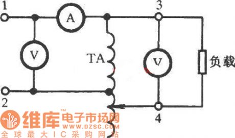
Voltage regulator voltage and load test is shown as in the picture. Make the AC input ends1 &2 of the voltage regulator connected to standard voltage of 220V; make the secondary ends 3 & 4 connected to AC voltmeter V; spin the voltage regulator hand wheel and then the secondary output voltage should rise to 250V from 0V. In processing load test, ends 1 & 2 are connected to standard voltage of 220V, and secondary 3 & 4 are connected to the load. For example, a voltage regulator of 1KVA can be connected to electric stove of 1KW and concatenated with AC voltmeter A. Spin the voltage regulator hand wheel , and then the current reaches rated current value of 4A and keep the power on for 2 hours. If no abnormal phenomena such as smoking and smell of burning arise, the quality of voltage regulator TA is good. (View)
View full Circuit Diagram | Comments | Reading(866)
Triode Performance Quick Test Circuit Diagram
Published:2011/6/26 9:22:00 Author:Vicky | Keyword: Triode Performance
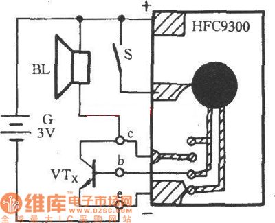
The picture above is a triode performance quick test circuit. In the picture, HFC9300 is a musical integrated circuit with a piece of music stored. BL is the speaker, and S is the triggering switch. VTx is triode under test. Insert it in a socket and insert the collector of the base in into ‘c’, the base into ‘b’ and emitter into ‘e’. If theVTx wokrs, BL would play a piece of touching music; otherwise, BL would give out no sound. (View)
View full Circuit Diagram | Comments | Reading(673)
Deep well water level probing and sucking device circuit diagram
Published:2011/6/25 10:46:00 Author:Vicky | Keyword: water level probing and sucking device
The circuit as shown in the above picture is composed of conductive sensor probe, electronic switch circuit, silicon-controlled control-motor circuit, croak-sounding circuit and AC brownout rectifying circuit. Its circuit is simple and It is very easy to test the water level and suction in a deep well. (View)
View full Circuit Diagram | Comments | Reading(1477)
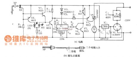
Ultrasonic Remote Switch Obbligato Sounding Circuit Diagram
Published:2011/6/25 10:45:00 Author:Vicky | Keyword: Ultrasonic Remote Switch Obbligato Sounding
The circuit in the above picture is composed by ultrasonic remote transmitter (picture a) and receiving and controlling sections. The circuit adpts 40KHz ultrasonic signal as the remote control command, with a effecting range of no less than 25m2. (View)
View full Circuit Diagram | Comments | Reading(673)
Capacitance Charge and Discharge Demonstrator Circuit Diagram
Published:2011/6/15 8:21:00 Author:Vicky | Keyword: Capacitance Charge and Discharge Demonstrator
Capacitance Charge and Discharge Demonstrator is mainly used to demonstrate the changing of the curves of voltage at the two ends of the capacitance and the discharge current as the pass of time when the capacitance is in the processions of charging and discharging. The following picture is a demonstration circuit. It adopts the way of displaying by the luminosity aroused by flow of the luminous diode, and it is vivid and visual , and very close to the actual procession of charging or discharging , which is of great practical value. (View)
View full Circuit Diagram | Comments | Reading(716)
One Digit Random Number Generator Circuit Diagram
Published:2011/6/15 8:14:00 Author:Vicky | Keyword: One Digit Random Number Generator
Random Number Generator is a digital generator which is not controlled by men's will.Thereforeit is fair and just to use it as Ernie (electronic random number indicator equipment). The working principle of random number generator is as shown in the picture. (View)
View full Circuit Diagram | Comments | Reading(2923)
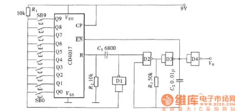
Diagram of 1 to 9 Pulse Selection Circuit
Published:2011/6/15 8:11:00 Author:Vicky | Keyword: Diagram of 1 to 9 Pulse Selection Circuit,
(View)
View full Circuit Diagram | Comments | Reading(739)
Arbitrary Number System Output Circuit Diagram
Published:2011/6/15 8:22:00 Author:Vicky | Keyword: Arbitrary Number System
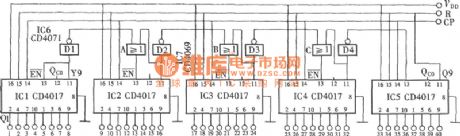
Output Circuit of arbitrary number system (View)
View full Circuit Diagram | Comments | Reading(722)
| Pages:88/101 At 2081828384858687888990919293949596979899100Under 20 |
Circuit Categories
power supply circuit
Amplifier Circuit
Basic Circuit
LED and Light Circuit
Sensor Circuit
Signal Processing
Electrical Equipment Circuit
Control Circuit
Remote Control Circuit
A/D-D/A Converter Circuit
Audio Circuit
Measuring and Test Circuit
Communication Circuit
Computer-Related Circuit
555 Circuit
Automotive Circuit
Repairing Circuit