
Signal Processing
Index 107
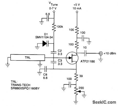
1700_MHz_VCO_CIRCUIT
Published:2009/7/22 3:37:00 Author:Jessie
This VCO circuit is for 1700 MHz and uses a ceramic coaxial resonator (View)
View full Circuit Diagram | Comments | Reading(2103)
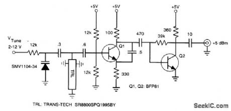
TRANSMISSION_LINE_RESONATOR_VCO_CIRCUIT
Published:2009/7/22 3:36:00 Author:Jessie
The figure shows a typical VCO circuit using a transmission-line resonator and varactor tuning. This circuit is for 855 to 890 MHz. (View)
View full Circuit Diagram | Comments | Reading(1248)
OSCILLATOR_CLOCK_GENERATOR
Published:2009/7/6 21:04:00 Author:May
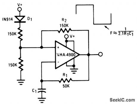
This self-starting fixed-frequency oscillator circuit gives excellent frequency stability. R1 and C1 comprise the frequency-determining network, while R2 provides the regenerative feedback.Diode D1 enhances the stability by compensating for the difference between VOH and VSUPPLY. In applications where a precision clock generator up to 100 kHz is required, such as in automatic test equipment, C1 might be replaced by a crystal. (View)
View full Circuit Diagram | Comments | Reading(1594)
100_Hz_CTCSS_OSCILLATOR
Published:2009/7/22 1:41:00 Author:Jessie
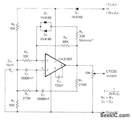
Stable Wien-bridge oscillator provides continuous-tone-coded subaudible squelch (CTCSS) for amateur FM repeater system to protect input from interference on commonly shared channels and add security to input frequency. Tone can be heard in background but does not become irritating. Use film resistors for R1 and R2. C1 and C2 should be polystyrene, polycarbonate, Teflon, or silver mica. Select R5 to give 8-10 V P-P sine wave when operating from 12-V supply. R1 and R2 may be varied slightly to adjust frequency.-D. Dauben, Miniature Solid State Tone Encoders to Replace Reeds, CQ, Dce. 1975, p 42-45 and 76. (View)
View full Circuit Diagram | Comments | Reading(1533)
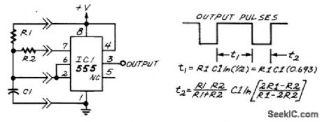
555_SQUARE_WAVE_GENERATOR
Published:2009/7/22 2:15:00 Author:Jessie
The 555 can be connected in either monostable or astable configurations, but for continuous square waves, the astable circuit is used. The square-wave signal appears at pin 3 of the 555. The out-put frequency of the 555 astable multivibrator is found from
ƒo=1.44/[(R1+2R2)C1]The duty cycle of the 555's square-wave output is determined by the relationship between R1 and R2, and is given by: Duty cycle=(R1+R2)/R2 (View)
View full Circuit Diagram | Comments | Reading(1321)
SQUARE_WAVE_OSCILLATOR
Published:2009/7/22 2:10:00 Author:Jessie
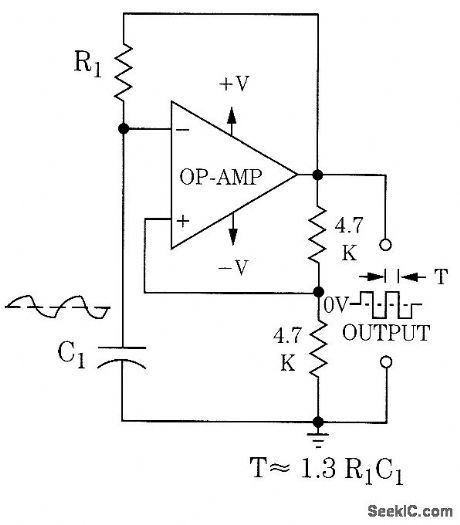
An op amp can be used as a square-wave generator, as shown. (View)
View full Circuit Diagram | Comments | Reading(278)
CMOS_INVERTING_SQUARE_WAVE_OSCILLATOR
Published:2009/7/22 2:08:00 Author:Jessie

This CMOS inverting square-wave oscillator can be varied over a wide range. Note that R2 should be 10 times the value of R1, as shown. IC can be a CMOS inverter, or else a NOR or NAND gate wired as an inverter. The frequency is approximately 1/(2.2R1,C1). (View)
View full Circuit Diagram | Comments | Reading(1122)
ARBITRARY_DUTY_CYCLE_SQUARE_WAVE_OSCILLATOR
Published:2009/7/22 2:07:00 Author:Jessie
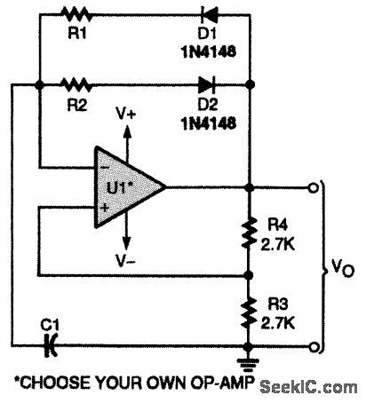
This op-amp-based square-wave generator uses diode switching to produce a fixed duty cycle other than 50 percent. (View)
View full Circuit Diagram | Comments | Reading(1825)
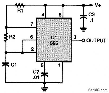
SQUARE_WAVE_OSCILLATOR_1
Published:2009/7/22 3:13:00 Author:Jessie
This circuit will produce a 50-percent duty cycle from a 555. (View)
View full Circuit Diagram | Comments | Reading(632)
SCHMITT_TRIGGER_RC_OSCILLATOR
Published:2009/7/22 2:26:00 Author:Jessie
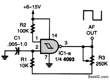
Here's another square-wave oscillator that uses a CMOS IC with input hysteresis. In this RC oscillator circuit, a single gate of a quad two-input NAND Schmitt-Trigger IC is the active element. (View)
View full Circuit Diagram | Comments | Reading(3325)
CD4047_CMOS_OSCILLATOR
Published:2009/7/22 2:21:00 Author:Jessie
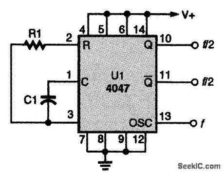
This CMOS square-wave oscillator is based on the 4047 multivibrator circuit, which can be used for either monostable ( one-shot ) or astable applications. In the configuration shown, the 4047 is an astable multivibrator. There are three outputs from the 4047. The first is the oscillator (OSC) output, which is connected directly to the internal oscillator circuit. The other two outputs, Q and Q, are complementary to each other and operate at one half the frequency of the internal oscillator. The output frequency is set by timing components R1 and C1:
ƒo=1/(4.4R1C1)
R1 should be between 10,000 Ω and 1 MΩ, while C1 should be 100 pF or more (the maximum capacitance is not limited theoretically, but a practical limit exists when the leakage resistance of C1 is of the same order of magnitude as R1). (View)
View full Circuit Diagram | Comments | Reading(10351)
RC_OSCILLATOR
Published:2009/7/22 2:17:00 Author:Jessie
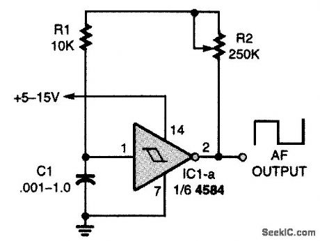
A single gate of a 4584 chip is connected in a simple RC square-wave audio-oscillator circuit. C1, R1, and R2 set the oscillator's frequency. The frequency range can be modified easily by changing the value of C1. The larger you make the capacitance, the lower the frequency range, and vice versa. Mylar, polystyrene, or a similar low-leakage capacitor works best in these high-impedance RC circuits. (View)
View full Circuit Diagram | Comments | Reading(1242)
Optocoupler_that_is_used_as_a_load_to_logic_translator
Published:2009/7/22 21:52:00 Author:Jessie
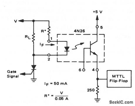
This circuit shows a 4N26 that is used to couple a high-voltage load to a low-voltage logic input. In this case, the value of R is chosen so that the output current is greater than 10 mA (to ensure that the 4N26 output voltage exceeds the logic-one level of the flip-flop). (View)
View full Circuit Diagram | Comments | Reading(1987)
NE602_VARACTOR_TUNED_COLPITTS_VFO
Published:2009/7/22 3:53:00 Author:Jessie
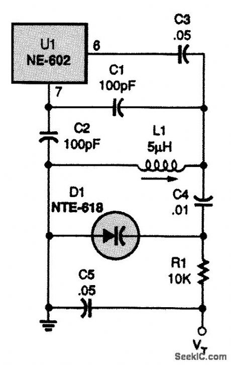
You can use a varactor diode (D1) to tune a VFO circuit electronically. This figure shows a parallel-resonant, voltage-tuned Colpitts oscillator. (View)
View full Circuit Diagram | Comments | Reading(1202)
VACKAR_VFO
Published:2009/7/22 3:50:00 Author:Jessie
This high-stability FET Vackar oscillator, covering 5.88 to 6.93 MHz, was developed by G3PDM in the late 1960s, but is still a valid design for HP VFOs for receiver, transmitter, and transceiver applications. (View)
View full Circuit Diagram | Comments | Reading(3192)
VFO_TUNING_CIRCUITS
Published:2009/7/22 3:50:00 Author:Jessie
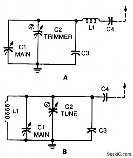
These are typical tuning circuits. The one in B is parallel resonant and the one in A is series resonant. (View)
View full Circuit Diagram | Comments | Reading(796)
NE602_VOLTAGE_TUNED_CLAPP_VFO
Published:2009/7/22 3:49:00 Author:Jessie

Here is a series-resonant, voltage-tuned Clapp oscillator circuit. (View)
View full Circuit Diagram | Comments | Reading(656)
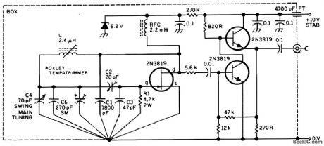
FSK_SQUARE_TRIANGLE_GENERATOR_
Published:2009/7/6 20:39:00 Author:May
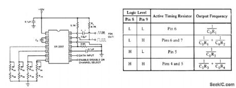
Uses Exar XR-2207 FSK modulator connected for single-supply operation, to produce triangle or square FSK outputs for either single-channel or two-channel multiplex operation. Used in transmitting digital data over telecommunication links. Table gives equations for selecting timing resistors R1-R4; resistor values are in ohms, C0is in farads, and frequency is in hertz. For optimum stability, R1 and R3 should be in range of 10K to 100K. For two-channel multiplex, make connections shown by dotted lines.- Phase-Locked Loop Data Book, Exar Integrated Systems, Sunnyvale, CA, 1978, p 57-61. (View)
View full Circuit Diagram | Comments | Reading(1429)
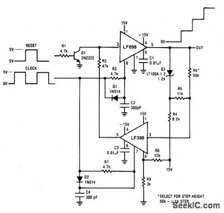
STAIRCASE_GENERATOR_Ⅱ
Published:2009/7/6 19:59:00 Author:May
View full Circuit Diagram | Comments | Reading(592)
STAIRCASE_GENERATOR
Published:2009/7/6 19:57:00 Author:May
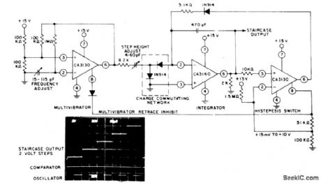
The circuit uses three BiMOS op amps. Two CA3130's are used, one as a multivibrator and the other as a hysteresis switch. The third amplifier, a CA3160, is used as a linear staircase generator. (View)
View full Circuit Diagram | Comments | Reading(4627)
| Pages:107/195 At 20101102103104105106107108109110111112113114115116117118119120Under 20 |
Circuit Categories
power supply circuit
Amplifier Circuit
Basic Circuit
LED and Light Circuit
Sensor Circuit
Signal Processing
Electrical Equipment Circuit
Control Circuit
Remote Control Circuit
A/D-D/A Converter Circuit
Audio Circuit
Measuring and Test Circuit
Communication Circuit
Computer-Related Circuit
555 Circuit
Automotive Circuit
Repairing Circuit