
Signal Processing
Index 112
CODE_PRACTICE_OSCILLATOR
Published:2009/7/5 22:59:00 Author:May
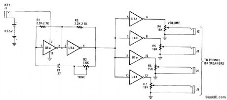
The inexpensive 7404 hex-inverter has enough amplification to handle a wide range of transducers. Closing the key completes the battery circuit and applies four to five volts to the 7404. Bias for the first two inverter amps (U1a and U1b) comes from the two resistors, R1 and R2, connected between their inputs and outputs. The capacitor and rheostat (R3/C1) close the feedback loop from the input to the properly-phased output.
The signal leaving Ulb drives the remaining four inverter amplifiers, U1c through U1f; they, in turn, drive the phones or speakers. The volume control potentiometers, R4-R7, may have any value front 1500 ohms to 10,000 ohms. The smaller values work best when speakers, or low impedance phones, are used. (View)
View full Circuit Diagram | Comments | Reading(0)
INEXPENSIVE_OSCILLATOR_IS_TEMPERATURE_STABLE
Published:2009/7/5 22:57:00 Author:May
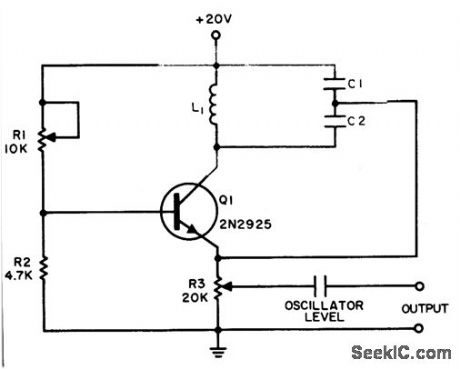
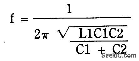
The Colpitts sinusoidal oscillator provides stable output amplitude and frequency from 0°F to +150°F. In addition, output amplitude is large and harmonic distortion is low. Oscillation is sustained by feedback from the collector tank circuit to the emitter. The oscillator's frequency is determined by:
Potentiometer R3 is an output level control.
Control R1 may be used to adjust base bias for maximum-amplitude output. The circuit was operated at 50 kHz with L1 = 10mH, C1 = 3500 pF, and C2 1500 pF.
(View)
View full Circuit Diagram | Comments | Reading(989)
1_kHz_OSCILLATOR
Published:2009/7/5 22:57:00 Author:May
If fine output control is desired, add the 10 K potentiometer. When the oscillator is connected to a dc circuit then connect a dc blocking capacitor in series with the potentiometer's wiper arm. (View)
View full Circuit Diagram | Comments | Reading(1461)
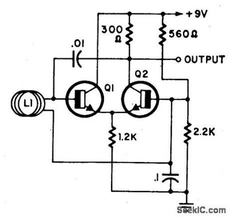
CASSETTE_BIAS_OSCILLATOR
Published:2009/7/5 22:55:00 Author:May
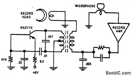
View full Circuit Diagram | Comments | Reading(729)
RESISTANCE_CONTROLLED_DIGITAL_OSCILLATOR
Published:2009/7/5 22:55:00 Author:May
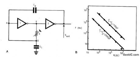
This very simple, low cost oscillator, is built with two CMOS buffer inverters, two capacitors and a variable resistance. The circuit can work with voltages ranging from 4 V up to 18 V. If C1 = C2, the frequency of oscillation, (ignoring the output and input impedance) is given by:
The graph in Fig. B shows how the output frequency varies with resistance when C1=C2=100 pF and C1=C2=2000 pF.
(View)
View full Circuit Diagram | Comments | Reading(789)
TUNABLE_FREQUENCY_OSCILLATORS
Published:2009/7/5 22:53:00 Author:May
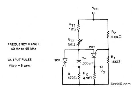
The variable oscillator circuit includes active elements for discharging the timing capacitor CT shown in Fig. 66-7A. A second method is given as in Fig. 66-7B (View)
View full Circuit Diagram | Comments | Reading(795)
SINGLE_CONTROL_FOUR_DECADE_VARIABLE_OSCILLATOR
Published:2009/7/5 22:52:00 Author:May
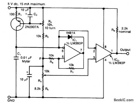
The circuit consists of a variable current Source that charges a capacitor, which is rapidly discharged by a Schmitt-trigger comparator, The sawtooth waveform thusproduced is fed to another comparator, one with a variable switching level. The outputfrom the second comparator is a pulse train with an independently adjustable frequencyand duty cycle. The variable-frequency ramp generator consists of capacitor C1, which is charged by a variable and nonlinear current source. The latter compnses a 2N2907A pnp transistor, plus resistor R1 and the potentiometer R2 Capacitor C2 eliminates any ripple or nolse at the base ofthe transistor that might cause frequency jitter at the output (View)
View full Circuit Diagram | Comments | Reading(1660)
4_MHz_NAND_GATE_OSCILLATOR_SYNCHRO_NIZES_TW0_MPUs_
Published:2009/7/5 22:50:00 Author:May
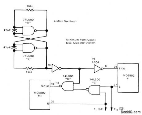
Low-cost NAND-gate sections A and B form low-cost oscillator for driving two Motorola MC6802 microprocessors.NAND gates C and D function as phase-locked loop, with D ensuring that phases of enable outputs are 180° apart. Small drifts in oscillator frequency do not affect synchronization. Circuit allows each MPU to operate during half-cycle that other MPU has disabled, to provide additional computing power of two microprocessors while maintaining system costs of onedata bus.-J. Farrell, Synchronizing Two Motorola MC6802s on One Bus, Motorola, Phoenix, AZ, 1978, AN-783. (View)
View full Circuit Diagram | Comments | Reading(1342)
ONE_SECOND,1_kHz_OSCILLATOR
Published:2009/7/5 22:49:00 Author:May
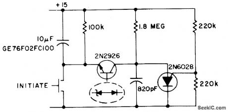
This circuit operates as an oscillator and a timer. The 2N6028 is normally on due to excess holding current through the 100 k resistor.
When the switch is momentarily closed, the 10 μF capacitor is charged to a full 15 volts and 2N2926 starts oscillating (1.8 M and 820 pF). (View)
View full Circuit Diagram | Comments | Reading(2344)
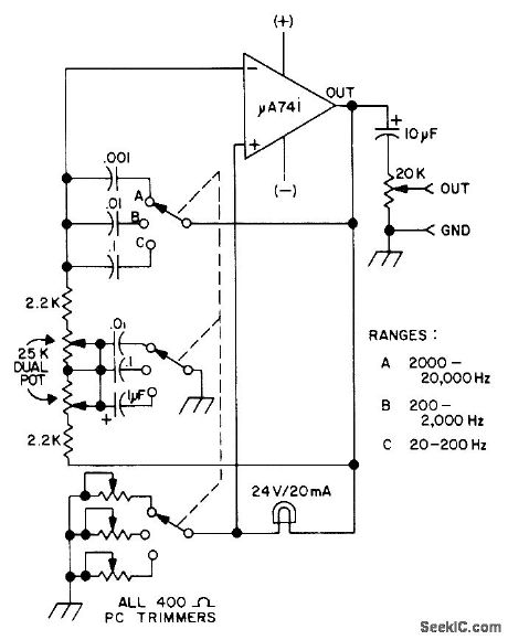
OSCILLATOR_ADJUSTABLE_OVER_10_1_RANGE
Published:2009/7/5 22:48:00 Author:May
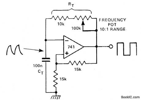
In this circuit, there are two feedback paths around an op amp. One is positive dc feedback which forms a Schmitt trigger. The other is a CR timing network. Imagine that the output voltage is +10V. The voltage at the noninverting terminal is +15V.
The voltage at the inverting terminal is a rising voltage with a time constant of CTRT.
When this voltage exceeds + 5V, the op amp's output will go low and the Schmitt trigger action will make it snap into its negative state. Now the output is - 10 V and the voltage at the inverting terminal falls with the time constant as before. By changing this time constant with a variable resistor, a variable frequency oscillation may be produced. (View)
View full Circuit Diagram | Comments | Reading(1447)
5_pF_TO_1μF
Published:2009/7/5 22:47:00 Author:May
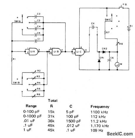
Consists of an oscillator using two gates from CD4011 quad NAND gate, separated from diode rectifier by another NAND gate. Increasing oscillator frequency gives more pulses per second and higher integrated meter reading. Each meter range is linear, so value of 5-pF capacitor can be read on lowest range.Diodes are 1N34 or equivalent. R1 is 12K, and R2-R6 are 50K trimpots set to values shown in table. R7 is 5K, and R8 is 10K trimpot. B1 is 9-V transistor battery. Article covers construction and calibration with known capacitors.-E. Landefeld, Build a Simple Capacitance Meter, 73Magazine, Jan. 1978, p 164-165. (View)
View full Circuit Diagram | Comments | Reading(1292)
1000_MC_NPN_OSCILLATOR
Published:2009/7/23 21:56:00 Author:Jessie
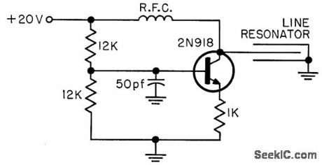
Can deliver over 2 mw, adequate for uhf tuner, and operate at temperatures up to 200℃.-Gigacycle Oscillator, EEE,10:12, p 102. (View)
View full Circuit Diagram | Comments | Reading(2006)
Model_control_receiver
Published:2009/7/23 21:55:00 Author:Jessie
This circuit shows the ZN414Z (Fig. 2-14A) used as an IF amplifier for a 27-MHz superhet receiver, such as those used in model remote-control systems. (View)
View full Circuit Diagram | Comments | Reading(1014)
TUNNEL_DIODE_TRANSMITTER
Published:2009/7/23 21:55:00 Author:Jessie

Can be frequency-modulated for remote-control applications. All components are mounted on body of piston-type trimmer capacitor. Tuning range is 50 to 250 Mc.-Tuner Elements Ride Piggyback, Electronics, 35:31, p 54-56. (View)
View full Circuit Diagram | Comments | Reading(1939)
EMITTER_COUPLED_BIG_LOOP_OSCILLATOR
Published:2009/7/5 22:45:00 Author:May
L1 is a loop of 10 to 20 turns of insulated wire with a diameter anywhere between 4 to 4'. Oscillator frequency (7 to 30 MHz) shifts substantially when a person comes near or into the loop. This oscillator together with a reso-nant detector might make a very good anti-personnel alarm. Transistors are 2N2926 or equivalent. (View)
View full Circuit Diagram | Comments | Reading(1032)
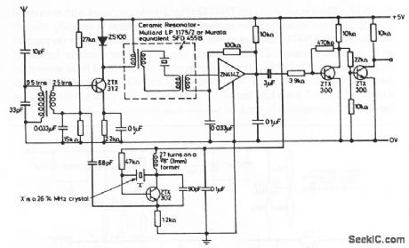
RF_GENIE
Published:2009/7/5 22:43:00 Author:May
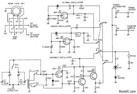
A variable oscillator covers 3.2 to 22 MHz in two bands-providing coverage of 80 through 15 meters plus most crystal-filter frequencies. Optional455 kHz and 10.7 MHz crystal oscillators can be switched on-line for precise tf alianmen' generator output is on the order of 4 volts p-p into a 500 ohm load. A simple voltage-divider attenuator controls the generator's output level, and a second output provides sufficient drive for an external frequency counter. (View)
View full Circuit Diagram | Comments | Reading(2291)
20_20000_Hz
Published:2009/7/5 22:42:00 Author:May
Wide-range audio oscillator covers AF spectrum in three switch-selected ranges, with harmonic distortion as low as 0.15%, for quick checks of audio equipment. Drain is only 6 mA from two 9-V batteries. Circuit is Wien-bridge oscillator using 741 opamp. Article covers construction and calibration, including optional connection for operation from single 9-V battery with AF output reduced to 2 V.-J. J. Schultz, Wide Range IC Audio Oscillator, 73 Magazine, Jan. 1974, p 25-28. (View)
View full Circuit Diagram | Comments | Reading(974)
SERIAL_ASCII_GENERATOR
Published:2009/7/5 22:39:00 Author:May
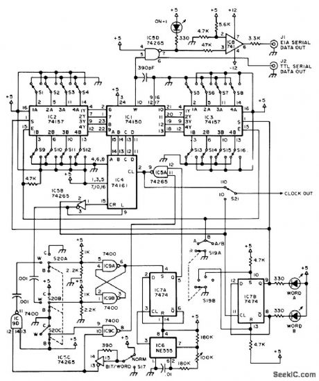
Provides choice of two different words in standard serial ASCII asynchronous data format for troubleshooting and testing code converters and other computer peripherals. S19 gives choice of four data output patterns. R gives logic high for all 8 bits.A gives pattern determined by settings of S1-S8. B gives pattern determined by settings of S9-S16. A/B alternates words A and B. S20 gives choice of three different output modes. Mode B generates words 1 bit at a time. Mode W produces single word at rate of 110 bauds. Mode C produces continuous output of selected word pattern, for testing teleprinters and other output devices. Article covers construction and operation of circuit. IC power (+5 V) and ground pins are: 74150-24 and 12; 74157, 74161, and 74265-16 and 8; 555-8 and 1; 7474 and 7400-14 and 7.-R. J. Finger, Build a Serial ASCII Word Generator, BYTE, May 1976, p 50-53. (View)
View full Circuit Diagram | Comments | Reading(1765)
DIGITAL_TRANSMISSION_ISOLATOR
Published:2009/7/5 22:32:00 Author:May
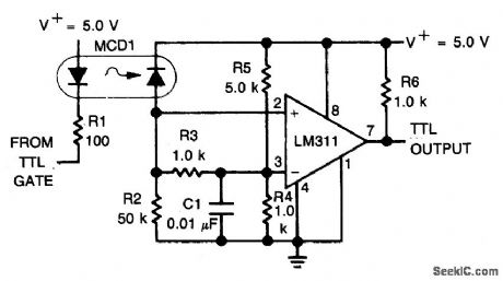
An optoelectronics device is used to couple a digital (TTL) signal to another system. The photodiode in the optocoupler drives an LM311 set up to produce a TTL compatible output. It is useful where grounds are not able to be connected for any reason. (View)
View full Circuit Diagram | Comments | Reading(0)
PRECISION_OSCILLATOR_TO_SWITCH_100_mA_LOADS
Published:2009/7/5 22:32:00 Author:May
View full Circuit Diagram | Comments | Reading(698)
| Pages:112/195 At 20101102103104105106107108109110111112113114115116117118119120Under 20 |
Circuit Categories
power supply circuit
Amplifier Circuit
Basic Circuit
LED and Light Circuit
Sensor Circuit
Signal Processing
Electrical Equipment Circuit
Control Circuit
Remote Control Circuit
A/D-D/A Converter Circuit
Audio Circuit
Measuring and Test Circuit
Communication Circuit
Computer-Related Circuit
555 Circuit
Automotive Circuit
Repairing Circuit