
Signal Processing
Index 103
FUNDAMENTAL_FR_EQUENCY_CRYSTAL_OSCILLATOR_2_60_PF_Qopendingon_Frquoncy_FREQUENCY_RANGE__1_0_N
Published:2009/7/7 7:04:00 Author:May
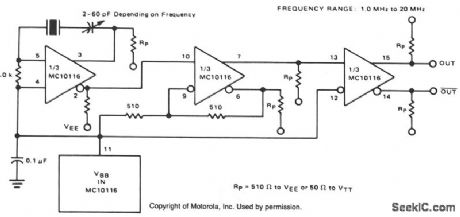
For frequencies below 20 MHz, a fundamental-frequency crystal can be used and the resonant tank is no longer required. Also, at this lower frequency range the typical MECL 10,000 propagation delay of 2 ns becomes small compared to the period of oscillation, and it becomes necessary to use a noninverting output. Thus, the MC10116 oscillator section functions simply as an amplifier. The 1.0 KΩ resistor biases the line receiver near VBBand the 0.1-μF capacitor is a filter capacitor for the VBB supply. The capacitor, in series with the crystal, provides for minor frequency adjustments. The second section of the MC10116 is connected as a Schmitt-trigger circuit; this ensures good MECL edges from a rather slow, less than 20-MHz input signal. The third stage of the MC10116 is used as a buffer and to give complementary outputs from the crystal oscillator circuit. The circuit has a maximum operating frequency of approximately 20 MHz and a minimum of approximately 1 MHz; it is intended for use with a crystal which operates in the fundamental mode of oscillation. (View)
View full Circuit Diagram | Comments | Reading(1494)
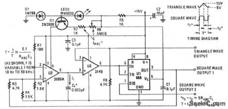
WIDE_RANGE_TRIANGLE__SQUARE_WAVE_GENERATOR
Published:2009/7/7 6:54:00 Author:May
View full Circuit Diagram | Comments | Reading(655)
PRECISE_TRIANGLE__SQUARE_WAVE_GENERATOR
Published:2009/7/7 6:52:00 Author:May
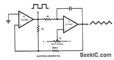
Since the output range swings exactly from rail to rail, frequency and duty cycle are virtually independent of power supply variations. (View)
View full Circuit Diagram | Comments | Reading(880)
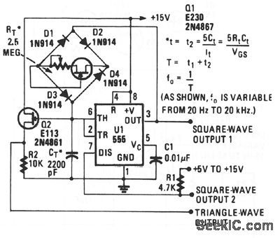
SAWTOOTH_AND_PULSE_GENERATOR
Published:2009/7/7 6:51:00 Author:May

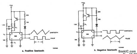
The pin 3 output of the 566 can be used to provide different charge and discharge currents for C1 so that a sawtooth output is available at pin 4 and a pulse at pin 3. The pnp transistor should be well saturated to preserve good temperature stability. The charge and discharge times can be estimated by using the formula:where RT is the combined resistance between pin 6 and VCC for the interval considered. (View)
View full Circuit Diagram | Comments | Reading(1616)
WIDE_RANGE_TUNABLE_FUNCTION_GENERATOR
Published:2009/7/7 6:49:00 Author:May
View full Circuit Diagram | Comments | Reading(703)
BASIC_FUNCTION_GENERATOR
Published:2009/7/7 6:48:00 Author:May
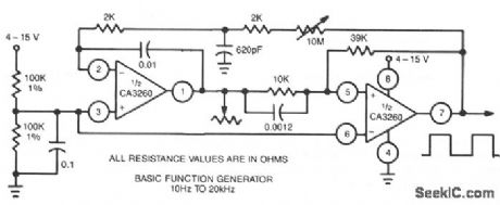
This function generator uses a CA3260 BiMOS Op amp to petform both the integrator and switchingfunctions.A 620-pF capacitor and 2-KΩ resistor shape feedback square wave to reduce spikes. Full audiospectrum, 10 Hz to 20 kHz,is covered with a single 10 Ω potentiometer. Requires 9-V battery. (View)
View full Circuit Diagram | Comments | Reading(876)
TRIANGLE__SQUARE_WAVE_GENERATOR
Published:2009/7/7 6:44:00 Author:May
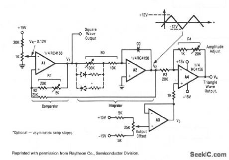
This circuit uses a positive-feedback loop closed around a combined comparator and integrator. When power is applied, the output of the comparator will switch to one of two states, to the maximum positive or maximum negative voltage. This applies a peak input signal to the integrator, and the integrator output will ramp either down or up, opposite of the input signal. When the integrator output, which is connected to the comparator input, reaches a threshold set by R1 and R2, the comparator will switch to the opposite polarity. This cycle will repeat endlessly, the integrator charging positive then negative, and the compara-tor switching in a square-wave fashion. (View)
View full Circuit Diagram | Comments | Reading(987)
SINGLE_CONTROL_FUNCTION_GENERATOR
Published:2009/7/7 6:42:00 Author:May
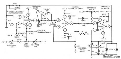

This function generator, with an adjustment range in excess of 1,000,000 to 1, uses a CA3160 BiMOS op amp as a voltage follower, a CA3080 OTA as a high-speed comparator, and a CA3080 as a programmable-current source. Three variable capacitors, C1, C2, and C3 shape the triangular signal between 500 kH and 1 MHz. Capacitors C4 and C5, and the trimmer potentiometer in series with C5, maintain essentially constant (±10%) amplitude to 1 MHz. (View)
View full Circuit Diagram | Comments | Reading(757)
FUNCTION_GENERATOR_1
Published:2009/7/7 6:32:00 Author:May
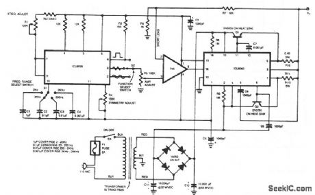
This generator will supply she, triangular, and square waves from 2 Hz to 20 kHz. This complete test instrument can be plugged into a standard 110 Vac line for power.VOUT will be up to ±25 V (50 V pk-pk across loads as small as 100 Ω about 2.5 A maximum output current).Capacitor working voltages should be greater than 50 Vdc and all resistors should be 1/2 W, unless otherwise indicated. The interconnecting leads from the 741 pins 2 and 3 to their respective resistors should be kept short, less than 2 inches if possible; longer leads might result in oscillation. Full output swing is possible to about 5 kHz; after that the output begins to taper off because of the slew rate of the 741, until at 20 kHz the output swing will be about 20Vpp ±10 V. This problem can be remedied by simply using an op amp with a higher slew rate, such as the LF356. (View)
View full Circuit Diagram | Comments | Reading(1900)
TRIANGLE_GENERATOR
Published:2009/7/7 6:25:00 Author:May
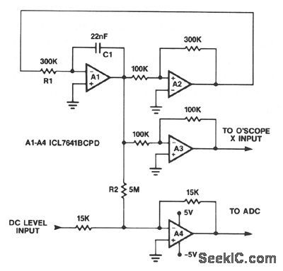
This circuit generates a symmetrical, 10-mV pk-pk triangle waveform which is summed with a dclevel and connected to the a/d analog input fornoise/DNL testing. The dc level input offsets thetriangle waveform over the input range of the ADC. The 10-mV amplitude amounts to an 8 LSB span for a 12-bit, 5-V. full-scale ADC. (View)
View full Circuit Diagram | Comments | Reading(839)
TWO_FUNCTION_SIGNAL_GENERATOR
Published:2009/7/7 6:24:00 Author:May
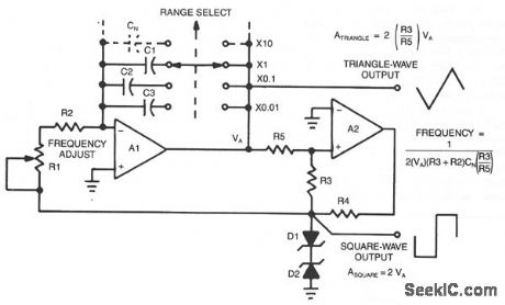
You can continously vary the frequencies of the triangle and square waves produced by this circuit over a full decade. If R5 = R3, the amplitude of the two waveforms will be equal (ASOUARE = ATRIANGLE). (View)
View full Circuit Diagram | Comments | Reading(678)
EASILY_TUNED_SINE_WAVE_SQUARE_WAVE_OSCILLATOR
Published:2009/7/7 6:18:00 Author:May
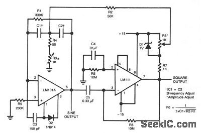
The circuit will provide both a sine- and square-wave output for frequencies from below 20 Hz to above 20 kHz. The frequency of oscillation is easily tuned by varying a single resistor. This is a considerable advantage over Wien-Bridge circuits where two elements must be tuned simultaneously to change frequency. Also, the output amplitude is relatively stable when the frequency is changed. An amp is used as a tuned circuit, driven by square wave from a voltage comparator. The frequency is controlled by R1, R2, C1, C2, and R3, with R3 used for tuning. Tuning the filter does not affect its gain or bandwidth, so the output amplitude does not change with frequency.A comparator is fed with the sine-wave output to obtain a square wave. The square wave is then fed back to the input of the tuned circuit to cause oscillation. Zener diode, D1, stabilizes the amplitude of the square wave fed back to the filter input. Starting is insured by R6 and C5 which provide dc negative feed-back around the comparator. This keeps the comparator in the active region. Distortion ranges between 0.75% and 2% depending on the setting of R3. Although greater tuning range can be accomplished by increasing the size of R3 beyond 1 KΩ, distortion becomes excessive. Decreasing R3 lower than 50 Ω can make the filter oscillate by itself. (View)
View full Circuit Diagram | Comments | Reading(947)
FOUR_STAGE_PNPN_BINARY_COUNTER
Published:2009/7/21 9:21:00 Author:Jessie
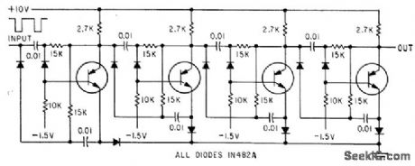
Operates on negative trigger pulses, to provide 16:1 division.-J. B. Hangsfefer and L. H. Dixon, Jr., Triggered Bistable Semiconductor Circuits, Electronics, 32:35, p 58-60. (View)
View full Circuit Diagram | Comments | Reading(727)
BLOCKING_OSCILLATOR_TRIGGER_GENERATOR
Published:2009/7/21 9:20:00 Author:Jessie
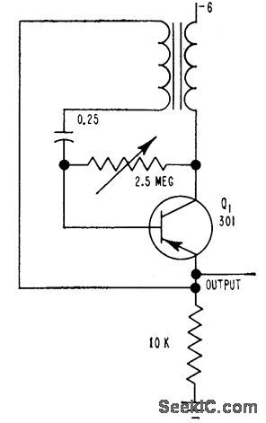
Generates relatively narrow pulses at adjustable repetition rate. Audio transformer provides positive feedback.-H. L. Armstrong, Transistorized Trigger and Delay Generators, Electronics, 313, p 96-98. (View)
View full Circuit Diagram | Comments | Reading(711)
COMBINATION_SCHMITT_MONOSTABLE
Published:2009/7/21 9:20:00 Author:Jessie
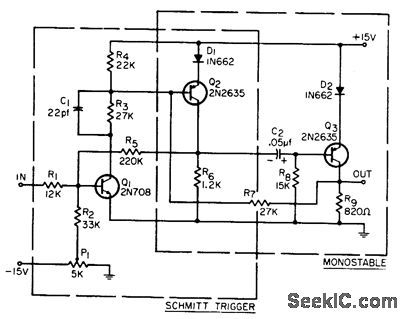
Three transistors in complementary connection give Schmitt trigger (Q1-Q2) und mono-stable mvbr (Q2-Q3) in which triggering level is accurately controlled. Output pulse width is independent of input because circuit is regenerative.-G. Marosi, Combination Schmitt Trigger-Monostable Multivibrator, EEE, 13:10, p 77. (View)
View full Circuit Diagram | Comments | Reading(854)
RANDOM_PULSE_DETECTOR
Published:2009/7/21 9:18:00 Author:Jessie
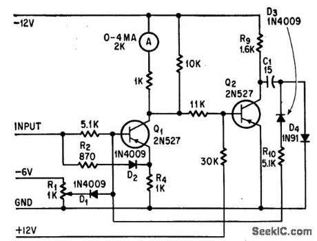
Either positive or negative pulses above predetermined minimum amplitude force Q1 into saturation and turn Q2 off, causing the meter to deflect immediately. Circuit may also be used as pulse stretcher or threshold detector.-C. F. Johnson and J. T. Loiselle, Bipolar Pulse Detector Features Meter Display, Electronics, 38:24, p 63. (View)
View full Circuit Diagram | Comments | Reading(708)
PULSE_GENERATOR
Published:2009/7/21 9:17:00 Author:Jessie
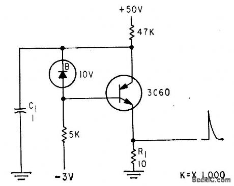
Delivers 1-amp peak out put current having duration of 10 microsec when pnpn unit is triggered on by low-level positive pulse applied to its base.-J. B. Hangstefer and L. H. Dixon, Jr., Triggered Bistable Semiconductor Circuits, Electronics, 32:35, p 58-60. (View)
View full Circuit Diagram | Comments | Reading(0)
SATURATED_TRANSISTOR_MEASUREMENT
Published:2009/7/21 9:16:00 Author:Jessie
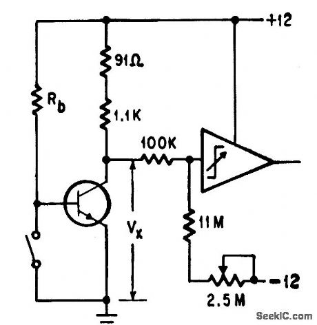
Transistor under lest is biased to saturate collector to within 100 my of ground for 10-ma collector load. Operational trigger then trips when Vx is 1 mv above 100 my.-P. Lefferts, Operational Trigger For Precise Control,Electronics,37:28,p 50-55. (View)
View full Circuit Diagram | Comments | Reading(762)
VARIABLE_HYSTERESIS_SCHMITT
Published:2009/7/21 9:15:00 Author:Jessie
R7 adjusts lower trigger point, and R8 adjusts upper trigger point.-R. S. Hughes, Variable-Hysteresis Schmitt Trigger, EEE, 13:7, p 41. (View)
View full Circuit Diagram | Comments | Reading(876)
HIGH_IMPEDANCE_SCHMITT
Published:2009/7/21 9:12:00 Author:Jessie
Use of let Q1 for input stage gives high input impedance, as required for threshold detector circuit. Output pulse is square wave at up to 100 kc triggering. Turnoff threshold is about 0.2 v below turnon.-L. R. Lott, FET Increases Schmitt Trigger Input Impedance, Electronics, 38:15, p 65. (View)
View full Circuit Diagram | Comments | Reading(1348)
| Pages:103/195 At 20101102103104105106107108109110111112113114115116117118119120Under 20 |
Circuit Categories
power supply circuit
Amplifier Circuit
Basic Circuit
LED and Light Circuit
Sensor Circuit
Signal Processing
Electrical Equipment Circuit
Control Circuit
Remote Control Circuit
A/D-D/A Converter Circuit
Audio Circuit
Measuring and Test Circuit
Communication Circuit
Computer-Related Circuit
555 Circuit
Automotive Circuit
Repairing Circuit