
Signal Processing
Index 105
THYRISTOR_TRIGGER_PULSE_GENERATOR
Published:2009/7/7 3:02:00 Author:May
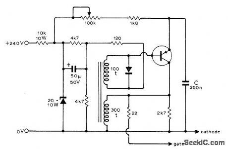
Used with thyristor speed control for 2-hp shunt-wound DC motor. Circuit provides train of pulses with variable delay with respect to zero-crossing instants of AC supply, for feeding to cathode and gate of thyristor to vary duty cycle. Use Mullard BFX29 silicon PNP transistor or equivalent, and any small-signal silicon diode. Output pulses are suitable for triggering all types of thyristors up to largest. Article also gives motor control circuit.-F. Butler, Thyris-tor Control of Shunt-Wound D.C. Motors, Wire-less World, Sept. 1974, p 325-328. (View)
View full Circuit Diagram | Comments | Reading(1963)
NEGATIVE_LOGIC_LAMP_DRIVER
Published:2009/7/21 22:25:00 Author:Jessie
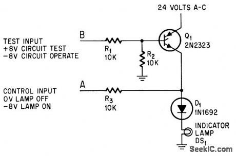
Uses one scr and only five components per lamp, to switch lamps rapidly, without relays or ex costive loading of control source. Positive test signal at B checks circuit and lamp, Control signal (-8 v) forward-biases gate electrode and scr fires during positive ac halfcycles.-A. E, Popodi, Reliable Repertoire Of Display Circuits, Electronics, 38:2, p 60-66. (View)
View full Circuit Diagram | Comments | Reading(813)
PULSE_TYPE_TRANSISTOR_TESTER
Published:2009/7/21 22:24:00 Author:Jessie

Constant-current drive for pulse-testing of power transistors at maximum power without over heating has three current ranges. A-c signal in phase with collector supply is advanced 88° by phase-shift bridge, to center one-shot mvbr pulse on peak of cc collector supply.-D. H. Breslow, Measuring Parameters by Power Transistor Pulse Techniques, Electronics, 34:1, p 120-122. (View)
View full Circuit Diagram | Comments | Reading(1098)
CARRIER_OSCILLATOR
Published:2009/7/21 22:20:00 Author:Jessie
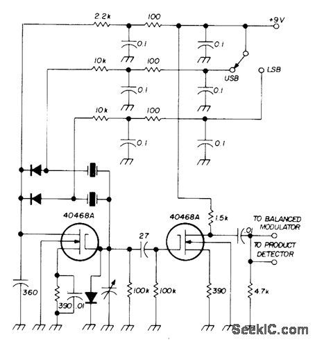
Two MOSFETs serve with diode switching arrangement for selecting either upper or lower sideband. Circuit between gates couples oscillator to isolating output stage. Upper/lower sideband switch applies +9V to anode of switching diode that closes feed-back circuit for crystal to be activated. Output can be used as injection voltage in demodulation of incoming signal by product detector of transceiver or as basic carrier applied to balanced modulator for transmitting mode. Used in SSB transceiver made by Sideband Associates for radio marine communication in 2-23 MHz range.-E. Noll, MOSFET Circuits, Ham Radio, Feb. 1975, p 50-57. (View)
View full Circuit Diagram | Comments | Reading(958)
CURRENT_PULSE_GENERATOR
Published:2009/7/21 22:19:00 Author:Jessie
Used for production testing of ferrite memory cores. Provides pulse amplitudes from 200 ma to 3 amp at repetition rates up to 20 kc.-H. W. Goss, Current Pulse Generator Tests Magnetic Cores, Electronics, 33:1, p 80-81. (View)
View full Circuit Diagram | Comments | Reading(1211)
TWO_TONE_BURSTS
Published:2009/7/21 22:19:00 Author:Jessie
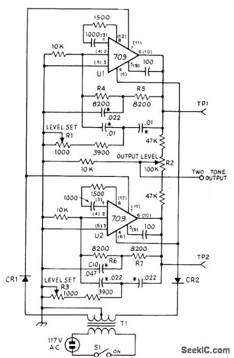
Uses 709 or 741 opamps to generate 1850-Hz and 855-Hz tones simulta-neously, pulsed at 60-Hz line rate for duty cycle slightly below 50%. Used to measure linearity of high-frequency amplifiers in low-power stages of SSB transmitter. Each opamp is pow-ered by half-wave rectified AC, with opposite voltage polarities provided by 12.6-V CT 50-mA filament transformer, Tone frequency of each opamp is determined by symmetrical twin-T network. R1 sets level of 1850-Hz tone, and R3 controls 855-Hz tone. R2 mixes and balances tones. Diodes are 50-PIV 500-mA silicon.-B. Buus, A Technique for Burst Two-Tone Testing of Linear Amplifiers, QST, Aug. 1971, p17-21. (View)
View full Circuit Diagram | Comments | Reading(687)
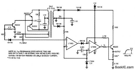
5V_POWERED_EEPROM_PULSE_GENERATOR
Published:2009/7/7 2:25:00 Author:May
View full Circuit Diagram | Comments | Reading(584)
PHASING_TYPE_SSB_GENERATOR
Published:2009/7/21 23:14:00 Author:Jessie
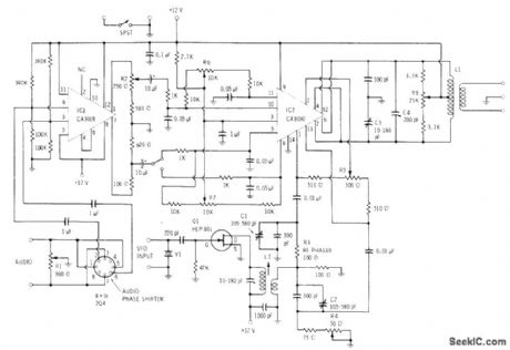
Modulating wave is first applied to input audio phase shifter for generating audio components that are equal in magnitude but differ 90°in phase. After amplification in CA3018, these audio components are applied to CA3050 double-balanced modulator. SPST and SPDT switch settings determine which sideband will appear at output of modulator. Carrier is generated by FET crystal oscillator for application through RF phase-shift network to pins 1 and 13 of modulator. Both carrier and modulating frequencies are suppressed in balanced output circuit of modulator, leaving only desired sideband. Resonant output transformer provides low-impedance feed to succeeding linear amplifier. Designed for 160-meter band.-E. M. Noll, Linear IC Principles, Experiments, and Projects, Howard W. Sams, Indianapolis, IN, 1974, p 356-357. (View)
View full Circuit Diagram | Comments | Reading(1582)
20_KC_WIRETRACING_PROBE
Published:2009/7/21 22:30:00 Author:Jessie
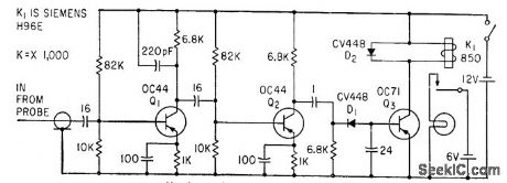
Used lo identify wire in middle of long cable, carrying 20-kc mvbr signal. Pickup probe for amplifier has 600 turns wound on U-shaped trans former steel. Relay doses and energizes lamp when probe is held near correct wire.-J. S. Rushton, Probe Identifies Catble Wiring, Electronics, 34:9, p 51. (View)
View full Circuit Diagram | Comments | Reading(686)
Time_sequencer_using_ECG955M_timer_oscillator_chips
Published:2009/7/21 22:30:00 Author:Jessie
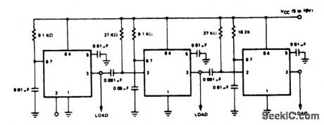
Time sequencer using ECG955M timer/oscillator chips. The first timer is started by momentarily connecting pin 2 to ground. It runs for 10 ms, then triggers the second timer. The second one runs for 50 ms, at which time it triggers the third. Note that the timing resistors and capacitors can be programmed and that each circuit could trigger several other timers (courtesy GTE Sylvania Incorporated). (View)
View full Circuit Diagram | Comments | Reading(828)
TRANSISTOR_TESTER_3
Published:2009/7/21 22:30:00 Author:Jessie
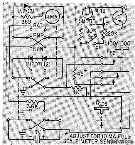
Leakage current and common-emitter current amplification are checked by using forward voltage drop across two silicon rectifiers in series as reference voltage. Base current of transistor under test is held constant by switching series base resistance.-G. F. Montgomery, Buildinga Simple Transistor Tester, Electronics, 36:16, p 56. (View)
View full Circuit Diagram | Comments | Reading(679)
FIXED_FREQUENCY_GENERATOR
Published:2009/7/7 1:25:00 Author:May
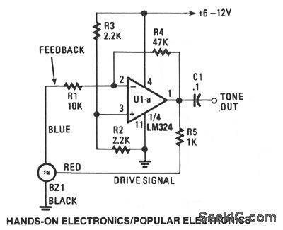
A single op amp, one fourth of an LM324 quad op amp, is configured as a standard inverting ampli-fter. At power up, a positive voltage is applied to the noninverting input of U1, via R3, forcing its output high. That high output travels along three paths. The first path is the tone output. Along the second path, by way of R5, that high is used as the drive signal for BZ1. In the third path, the high output of U1 is fed back, via R4, to the inverting input of U1. That forces U1's output to go low. And that low, when fed back to the inverting input of U1, causes the op amp output again to a high, and the cycle repeats itself. As configured, U1 provides a voltage gain of 4.7 (gain R4/R1).The outer ring of the piezo element is usually connected to the circuit ground. The large inner cir-cle serves as the driven area, and the small elon-gated section supplies the feedback signal. Resistor R5 sets BZ1's output-volume level. That level can be increased by decreasing R5 for example, to 470 Ω. To decrease the volume, increase R5 to about 2.2 KΩ, or so.Resistors R2 and R3 set the bias for op amp ,U1's positive input pin 3 to half of the supply-voltage level. That allows for a maximum voltage swing at U1's output. Although a quad op amp is specifted, almost any similar low cost single or dual op amp will work for U1a. (View)
View full Circuit Diagram | Comments | Reading(2181)
FILTER_TYPE_SSB_GENERATOR
Published:2009/7/21 22:47:00 Author:Jessie
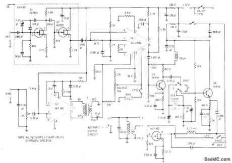
Carrier is generated by FET crystal oscillatorQ1 followed by buffer Q2. Modulating wave is applied to HEP 580 connected as two-stage audio amplifier feeding double-balanced modulator IC1 through transformer T1. Double-sideband signal from pin 6 of IC1 is applied to amplifier Q3-Q4 for straight-through amplification when double-sideband output is desired. For 9-MHz single-sideband operation, sideband filter is switched in between transistors.-E, M, Noll. Linear IC Principles, Experiments, and Projects. Howard W Sams, Indianapolis,IN,1974,p353-356. (View)
View full Circuit Diagram | Comments | Reading(1077)
VERSATILE_2φ_PULSE_GENERATOR
Published:2009/7/7 1:22:00 Author:May
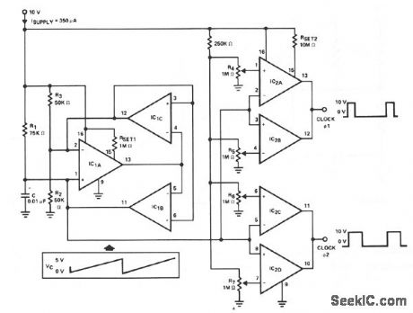
View full Circuit Diagram | Comments | Reading(812)
PRECISION_AUDIO_WAVEFORM_GENERATOR
Published:2009/7/7 1:19:00 Author:May
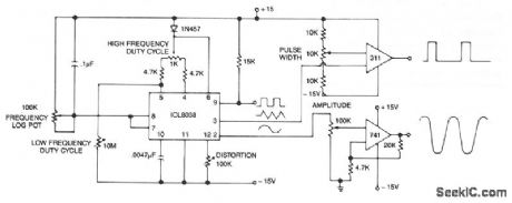
This circuit generates sinusoidal, square, and triangle waveforms simultaneously. Set the frequency to a particular value or vary it, as shown above. An op amp can be added for extra drive capability and simpli-fied amplitude adjustment. A simple comparator, slicing the triangle waveform, provides continuous duty cycle adjustment at a constant frequency. (View)
View full Circuit Diagram | Comments | Reading(1172)
CLIPPER
Published:2009/7/21 22:44:00 Author:Jessie
Combined speech amplifier and logarithmic clipper for use with SSB transmitters reduces speech bandwidth to about 500-3000 Hz, with very little distortion. Power can be obtained from separate battery or from transmitter itself.-Circuits, 73 Magazine, March 1977, p 152. (View)
View full Circuit Diagram | Comments | Reading(1944)
LOW_FREQUENCY_FM_GENERATORS
Published:2009/7/7 1:14:00 Author:May
Here are two FM generators for low frequency, less than 0.5 MHz center frequency, applications. Each uses a 566 function generator as a modulation generator and a second 566 as the carrier generator. Capacitor C1 selects the modulation frequency adjustment range and C1 selects the center frequency. Capacitor C2 is a coupling capacitor which only needs to be large enough to avoid distorting the modulating waveform. If a frequency sweep in only one direction is required, the 566 ramp generators given in this section can be used to drive the center generator. (View)
View full Circuit Diagram | Comments | Reading(1135)
HARMONICS_GENERATOR
Published:2009/7/7 1:12:00 Author:May
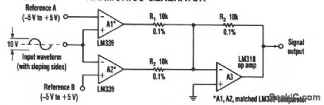
Two comparators and a summing amplifier that generate differential harmonic spectra comprise a sim-ple frequency multiplier. The resulting circuit can extract harmonics from a sine, triangle, sawtooth, or any other sloping-sided waveform. With a sloped-input waveform, a comparator produces an output pulse width that's proportional to the input amplitude plus a reference voltage. Changing the reference can vary the pulse width from 0 to 100%. As the pulse width changes, the harmonic spectrum changes, but two comparators combined in the adder eliminate harmonics, depending on the duty cycle. For example, a 50% pulse will lack all the even-num-bered harmonics. Similarly, a 25% duty-cycle pulse will be missing multiples of the fourth harmonic and deliver the second, sixth, and tenth harmonics. Accordingly, the circuit generates multiples of the input frequency that might not have existed in the input waveform. Adjusting the references can create virtually any harmonic. Because comparators A1 and A2 supply differential inputs to the added A3, the adder cancels out equal harmonics. Therefore, both A1 and A2 should have identical ac characteristics, and A3 should have good common-mode rejection and a high slew rate. In particular, R1, R2, and R3 should match within 0.1%. Of course, the accuracy of the circuit depends heavily on the amplitude stability of the input. (View)
View full Circuit Diagram | Comments | Reading(1082)
POWER_TRANSISTOR_TEST_GATE
Published:2009/7/21 22:32:00 Author:Jessie
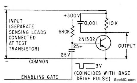
Rectangular pulse opens saturated amplifier; gate output is then ct series of pulses whose amplitude is equal to voltage across power transistor under lest when full load current is drawn.-D. H. Breslow, Measuring Parameters by Power Transistor Pulse Techniques, Electronics, 34:1, p 120-122. (View)
View full Circuit Diagram | Comments | Reading(765)
LOW_COST_FSK_GENERATOR
Published:2009/7/7 1:07:00 Author:May
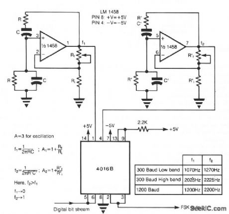
In FSK, two discrete frequencies are used to represent the binary digits0 and 1. The heart of the circuit consists of two Wien-bridge oscillators built using a dual op amp LM 1458, for the two frequencies. The two frequencies are enabled corresponding to digital data using two switches in SCL 4016. The control lines of these switches are logically inverted with respect to each other using one of the switches in SCL 4016 as an inverter, so as to enable only one oscillator output at a time. The digital bit stream is used to control the analog switches as shown. Since the switching frequency limit of SCL 4016 is 40 MHz, high-data rates can be easily accommodated. This method comes in handy when expensive FSK generator chips are not readily available; also, the components used in this circuit are easily available off the shelf and are quite cheap. (View)
View full Circuit Diagram | Comments | Reading(1158)
| Pages:105/195 At 20101102103104105106107108109110111112113114115116117118119120Under 20 |
Circuit Categories
power supply circuit
Amplifier Circuit
Basic Circuit
LED and Light Circuit
Sensor Circuit
Signal Processing
Electrical Equipment Circuit
Control Circuit
Remote Control Circuit
A/D-D/A Converter Circuit
Audio Circuit
Measuring and Test Circuit
Communication Circuit
Computer-Related Circuit
555 Circuit
Automotive Circuit
Repairing Circuit