
Signal Processing
Index 106
XOR_GATE_COMPLEMENTARY_SIGNALS_GENERATOR
Published:2009/7/7 1:05:00 Author:May
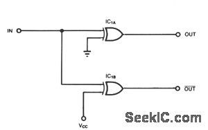
Some applications, such as driving three-state buffers for data multiplexers or for biphase clocks in high-speed systems, require complementary signals having a small-time skew and nearly simultaneous transitions. Here, XOR gates function as both inverting and noninverting gates. For CMOS systems, practically any type of XOR gate will work. However, the advanced-CMOS logic (ACL) families have the greatest drive capability, the shortest gate delays, and the tightest manufacturing tolerances. For TTL systems, compatible CMOS types such as the ACT or S/AS86 families are preferable. Do not use low-power TTL versions (LS or ALS), because they have large propagation delay differences when one XOR gate is inverting and the other is noninverting. (View)
View full Circuit Diagram | Comments | Reading(760)
PROGRAMMABLE_TRIANGLE__SQUARE_WAVE_GENERATOR
Published:2009/7/7 1:02:00 Author:May
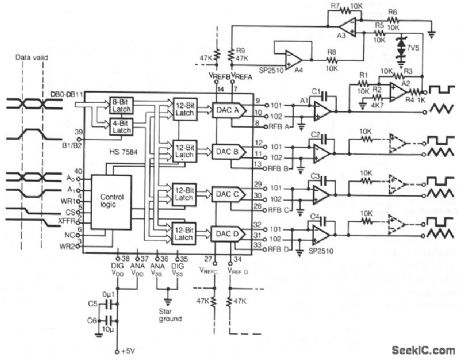
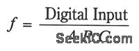
The programmable multiple output generator provides the control signals for data converter ATE. Major performance criteria are simple, interfaces to a number of microprocessor systems, low power con-sumption, stable output timing relationships combined with a minimum of board space. For schematic sim-plicity only, one output circuit is shown in full.The monolithic HS7584 provides four current output DAC's with four quadrant multiplication, individ-ual reference input and a feedback resistor. The digitally controlled integrator's frequency is determined by:C is the value of C1 to C4 andfi is the resistance of the DAC. With the four DACS on a single chip, the resistance matching is good, which results in stable timing relationships of the generator outputs. The out-put of the comparator A2 determines whether the constant current source provided by A3 and A4 is posi-tive or negative. (View)
View full Circuit Diagram | Comments | Reading(1063)
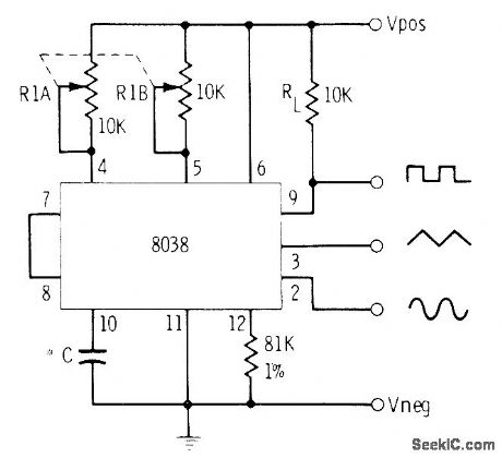
FUNCTION_GENERATOR
Published:2009/7/7 0:59:00 Author:May
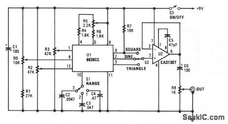
This circuit can output sine, square, and triangular signals of from 15 Hz to 25kHz in three ranges. The circuit is built around an 8038 function generator that produces the triangular- and square-wave out-puts directly from an oscillator. The triangular output is then processed to develop the sine waze. While that method doesn't provide a sufficiently low level of distortion to let you make distortion measurements on audio gear, the degree of purity is high enough for frequency-response tests and a lot of other audio analysis. Three switched capacitors, C2 to C4, set the circuits frequency range via switch S1. Variable resistor R9 and resistor R1 provide the voltage for controlling the charge and discharge rates of the timing capacitor selected. Resistors R4 to R6 control the charge and discharge currents. Resistor R5 can be adjusted to provide a 1.1 mark/space ratio. (View)
View full Circuit Diagram | Comments | Reading(0)
FOUR_OUTPUT_WAVEFORM_GENERATOR
Published:2009/7/7 0:57:00 Author:May
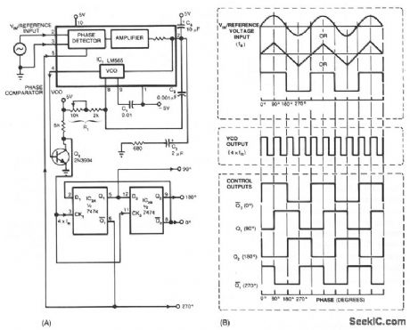
Many applications require control signals that have phase shifts with reference to an input signal. Circuit acceptsa sine, square, or triangular wave as an input reference signal and produces square-wave out-puts with 0°, 90°, 180°,and 270° phase shifts with respect to the input. Figure 38-3B shows the input and output waveforms. The circuit contains two ICs: an LM565 phase-locked loop and a 7474 dual-D posi-tive edge-triggered flip-flop. R1 and C1 set the free-running frequency of the LM565's VCO. You should adjust RI so that the frequency is approximately four times that of the input reference signal. The LM565 responds to input signals greater than 10 mV pk-pk; 3 V pk-pk is the,hipb maximum allowable input level. Q1 matches the LM565's output to the flip-flops' inputs. The flip-flops' outputs provide the TTL-compati-ble square-wave signals with 0°, 90°, 180°, and 270° phase shift with reference to the input signal. (View)
View full Circuit Diagram | Comments | Reading(2133)
LOUD_BIKE_SIREN
Published:2009/7/22 0:01:00 Author:Jessie
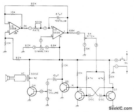
Uses 5558 dual opamp and four general-purpose NPN transistors to generate triangle wave that can be distorted by 10k symmetry control to give either fast or slow rise for sawtooth applied as base bias to astable MVBR Q1-Q2. Drain is reasonably low with 9-V radio battery, Repetition rate can be varied from long wail to rapid warble, and volume changed from soft to annoying. Article gives construction details, and recommends use of removable mounting on bike to avoid theft.-R. Megirian, Simple Electronic Siren, 73 Magazine, Oct.1977.p176-177. (View)
View full Circuit Diagram | Comments | Reading(918)
SQUARE_TRIANGLE_VCO
Published:2009/7/6 23:42:00 Author:May
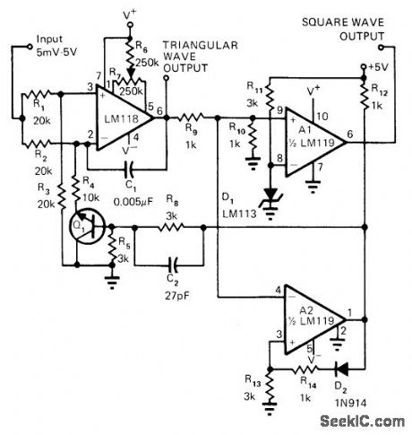
With DC control voltage of 5 mV to 5 V, circuit controls frequency of both square and triangle outputs with good linearity. Peak value of triangle output is precisely set at 2.44 V and 0 V by reference voltages at noninverting inputs of comparators.Comparator A2 drives load for low outputs, while comparator A1 drives load when output is high. Article tells how circuit works.-R. C.Dobkin, Comparators Can Do More Than Just Compare, EDN Magazine, Nov. 1, 1972, p 34-37. (View)
View full Circuit Diagram | Comments | Reading(1180)
HYPERBOLIC_SINE
Published:2009/7/6 23:27:00 Author:May
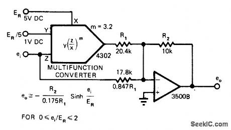
Burr-Brown 4302 multifunction converter and opamp generate hyperbolic sine transfer function with response matching ideal curve within 0.7%. Technique permits setting powers and roots at fractional as well as integer values. Converter shown is set for exponent of 3.2. Choice of amplifier gain and ref erence voltage scales response for given input and output signal levels. Article gives design equations.-J. Graeme, Sinh Generator Boasts 0.7% Error, END Magazine, Aug. 5, 1978, p 70 and 72. (View)
View full Circuit Diagram | Comments | Reading(995)
90_900Hz_SINE_SQUARE_TRIANGGLE_
Published:2009/7/6 23:22:00 Author:May
Ganged 10K dual pot covers range when C is 0.25 μF for 8038CC waveform generator. Other values of C (from 0.005,μF to 2.2 μF) give different frequency langes between 10 Hz and 50 kHz. Linearity of waveforms depends on tracking precision of dual pot.-C. D. Rakes, Integrated Circuit Projects, Howard W. Sams, lndianapolis, IN, 1975, p 116-120.
(View)
View full Circuit Diagram | Comments | Reading(829)
SIMPLE_TWO_TONE_GENERATOR
Published:2009/7/6 22:11:00 Author:May
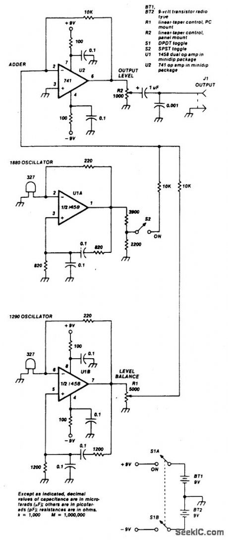
Circuit Notes
Two 741 operational amplifiers are used for the active element in this Wien bridge oscillator.(The 1458 is the dual version of the 741.) Frequencies of the two oscillators were chosen to fit standard component values. Other frequencies between 500 and 2000 Hz can be employed. They should not be harmonically related. The output level of U1A is set by a resistive divider, while the output of U1B is adjustable through R1. The output of the two oscillators is combined in U2, an op-amp adder with unity gain. The output from U2 can be adjusted using R2. (View)
View full Circuit Diagram | Comments | Reading(963)
ONE_IC_AUDIO_GENERATOR
Published:2009/7/6 22:06:00 Author:May
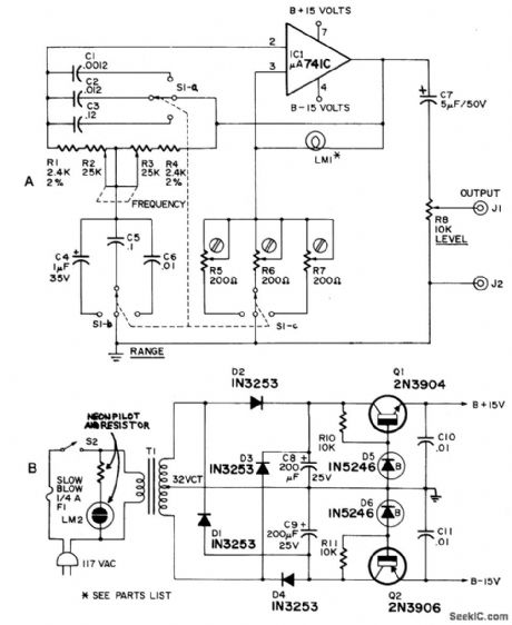
Circuit NotesThis high-quality low-cost generator covers 20 Hz to 20 kHz in three bands with less than 1% distortion. LM1-10 V, 14 mA (344, 1869, 914) or 10 \/, 10 mA (913, 367).
A = oscillatorB = power Supply (View)
View full Circuit Diagram | Comments | Reading(698)
ADJUSTABLE_SINE_WAVE_AUDIO_OSCILLATOR
Published:2009/7/6 22:01:00 Author:May
Circuit Notes
Waveform purity at low frequencies for a Wien bridge oscillator is enhanced by diode limiting. Lamp L1 stabilizes the loop gain at higher frequencies while the limiting action of R2, CR1, and CR2 prevents clipping at low frequencies and increases the frequency adjustment range from about 3:1 to greater than 10:1. (View)
View full Circuit Diagram | Comments | Reading(715)
A_555_USED_AS_AN_RC_AUDIO_OSCILLATOR
Published:2009/7/6 21:57:00 Author:May
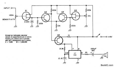


Circuit Notes
Transistor Q5 and the 1000 ohm resistor form the variable element needed for controlling the frequency of VDO by limiting the charging current flowing into the 0.15μF timing capacitor according to the forward bias being applied to Q5. As the voltage on pins 2 and 6 of U1 reach 2/3 VCC (about 6 volts with a 9-volt supply) the timer will fire and pin 3 will be pulled low. Pin 7, an open collector output, goes low and begins to discharge the timing capacitor-through the 3.3 kilohm resistor. The discharge time provided by this resistor assures a reasonable, although asymmetrical, waveform for the aural signal generated by U1. At 1/3 VCC the intemal flip-flop resets, the output on pin 3 goes high, the open collector output on pin 7 floats, and the timing cycle begins again. (View)
View full Circuit Diagram | Comments | Reading(1045)
LOW_COST_WIEN_BRIDGE_OSCILLATOR
Published:2009/7/6 21:51:00 Author:May
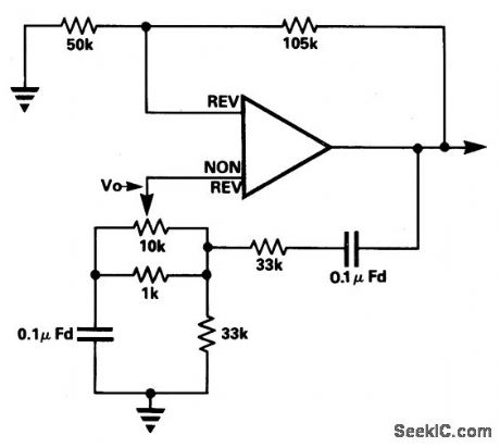

Circuit Notes
In the circuit the frequency trimming component is arranged so that the voltage across it is in quadrature with the voltage V, from the bridge so that as it is adjusted the attenuation of the bridge only changes a little, avoiding the need for a two gang component. The range of variation of frequency is very limited. By using a high gain amplifier and metal film feedback resistors the loop gain can be set so that the unit just oscillates and the use of an automatic gain setting component, a thermistor for example, is eliminated. (View)
View full Circuit Diagram | Comments | Reading(1287)
SIMPLE_AUDIO_SINE_WAVE_GENERATOR
Published:2009/7/6 21:45:00 Author:May
Circuit Notes
U1A, an op amp, oscillates at the frequency at which the phase shift in the Wien bridge network is exactly zero degrees. Changing bridge component values changes the oscillator frequency. In this circuit, we need change only the two resistors to do this. S1A chooses a value among R1 through R6, and S1B similarly selects a value from R7 through R12. U1A must provide enough gain to overcome losses in the bridge, but not so much gain that oscillation builds up to the point of overload and distortion. U2 andC1 automatically regulate circuit gain to maintain oscillation. U2 places D1 across R13 with the proper polarity on both positive and negative alterations of the signal at pin 1 of U1. As the voltage at pin 1 of U1 approaches its peak value, D1 enters its Zener breakdown region, effectively shunting R13 with a resistive load. This increases the amount of negative feedback around U1, reducing its gain. R15, WAVEFORM ADJ, allows you to optimize circuit operation for lowest distortion. U1B provides isolation between oscillator and load. With the values shown for R17 and R18, U1B operates at unity gain. (View)
View full Circuit Diagram | Comments | Reading(1735)
PULSE_SAWTOOTH_GENERATOR
Published:2009/7/6 21:42:00 Author:May
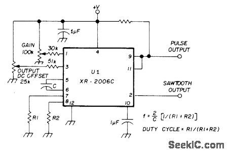
Pulse output is obtained from Exar XR-2006C functiongenerator l0 when pin 9 is shorted to squarewave output at pin 11. Pulse duty cycle, along with rise and fall times of ramp from pin 2, is determined by values of R1 and R2. Both can be adiusted from 1 to 99% by proper selection of resistor values as given in formulas alongside diagram.-E. NoLL VHF/UHF Single-Frequency Conversion, Ham Radio, April 1975, p 62-67. (View)
View full Circuit Diagram | Comments | Reading(915)
Basic_UJT_relaxation_oscillator
Published:2009/7/22 0:49:00 Author:Jessie
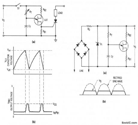
This figure shows the circuit and corresponding waveforms for a unijunction transistor oscillator (Fig. 5-41). When Vs is pure dc, the oscillator is free-running and RT/CT determine the frequency of oscillation. Figure 9-1B shows the basic relaxation oscillator, whore the output pulses are synchronized to the line-voltage zero-crossing points. Typical values (for a UJT with a base-to-base voltage of 4 to 9 V) are:RB1=40 to 100 Ω, RB2 1 kΩ, CT=0.1μF, RT= 100 kΩ. (View)
View full Circuit Diagram | Comments | Reading(2180)
CALIBRATING_MARK_SPACE_VCO
Published:2009/7/6 21:32:00 Author:May
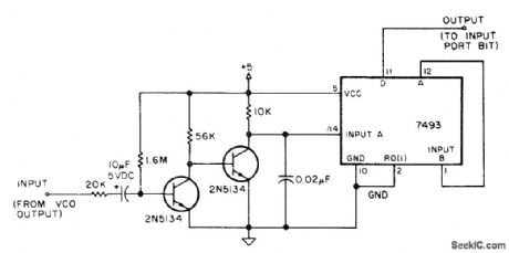
Simple buffer/counter provides accurate calibration of FSK circuit used in cassette interface of 8080 microprocessor to generate mark and space frequencies. Audio FSK waveform is squared and divided down in 7493 4-bit counter. Resulting pulses are fed to input port of microprocessor for software pulse counting. Software sets VCO frequency, waits until pulse starts, counts each pulse occurrence, and displays resultant count.Each 7493 count is 29 Hz or 14.5μs, so 371 counts correspond to 2975 Hz for space. Mark frequency of 2125 Hz gives pulses separated by 519 counts.-D. R. Bourdeau, Cassette Interface First Aid, Kilobaud, July 1977, p 49. (View)
View full Circuit Diagram | Comments | Reading(1600)
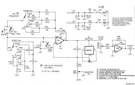
AUDIO_OSCILLATOR
Published:2009/7/6 21:26:00 Author:May
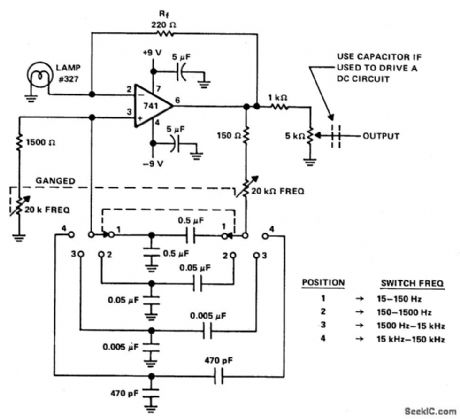
Circuit Notes
A Wien bridge oscillator produces sine waves with very low distortion level. The Wien bridge oscillator produces zero phase shift at only one frequency (f=1/2π RC) which will be the oscillation frequency. Stable oscillation can occur only if the loop gain remains at unity at the oscillation frequency. The circuit achieves this control by using the positive temperature coefficient of a small lamp to regulate gain (Rf/RLAMP) as the oscillator attempts to vary its output. The oscillator shown here has four frequency bands covering about 15 Hz to 150 kHz. The frequency is continuously variable within each frequency range with ganged 20 k ohm potentiometers. The oscillator draws only about 4.0 mA from the 9-V batteries. Its output is from 4 to 5 V with a 10 k ohm load and the Rf (feedback resistor) is set at about 5% below the point of clipping. As shown, the center arm of the 5 k ohm output potentiometer is the output terminal. To couple the oscillator to a dc type circuit, a capacitor should be inserted in series with the output lead. (View)
View full Circuit Diagram | Comments | Reading(0)
LOW_DISTORTION_SINE_WAVE_OSCILLATOR
Published:2009/7/6 21:22:00 Author:May
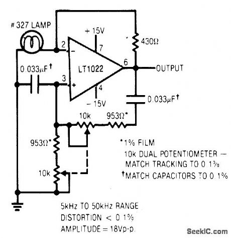
View full Circuit Diagram | Comments | Reading(0)
NE602_VOLTAGE_TUNED_LOCAL_OSCILLATOR_CIRCUITS
Published:2009/7/22 3:39:00 Author:Jessie
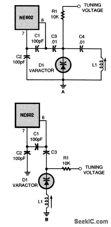
The LO circuit for the NE602 can also be voltage controlled. Here are two different voltage-tuned local-oscillator circuits. (View)
View full Circuit Diagram | Comments | Reading(711)
| Pages:106/195 At 20101102103104105106107108109110111112113114115116117118119120Under 20 |
Circuit Categories
power supply circuit
Amplifier Circuit
Basic Circuit
LED and Light Circuit
Sensor Circuit
Signal Processing
Electrical Equipment Circuit
Control Circuit
Remote Control Circuit
A/D-D/A Converter Circuit
Audio Circuit
Measuring and Test Circuit
Communication Circuit
Computer-Related Circuit
555 Circuit
Automotive Circuit
Repairing Circuit