
Amplifier Circuit
Index 3
By an order bandpass filter of an operational amplifier circuit diagram
Published:2014/3/24 21:27:00 Author:lynne | Keyword: By an order bandpass filter of an operational amplifier circuit diagram
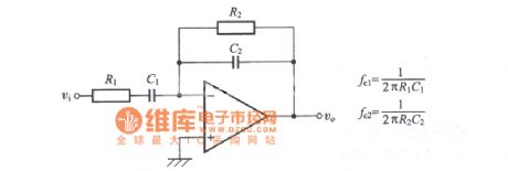
By an order bandpass filter of an operational amplifier circuit diagram as shown:
(View)
View full Circuit Diagram | Comments | Reading(1666)
Using operational amplifier low-pass filter circuit diagram
Published:2014/3/24 21:22:00 Author:lynne | Keyword: Using operational amplifier low-pass filter circuit diagram

Using operational amplifier low-pass filter circuit diagram as shown:
Let R1 = R2, then the gain of the low frequency range 1 (= 0db). (View)
View full Circuit Diagram | Comments | Reading(1612)
Reverse amplification circuit diagram
Published:2014/3/23 21:06:00 Author:lynne | Keyword: Reverse amplification circuit diagram
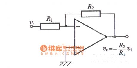
Reverse amplification circuit diagram as shown:
(View)
View full Circuit Diagram | Comments | Reading(1362)
Zero-drift operational amplifier circuit diagrams
Published:2014/3/20 21:04:00 Author:lynne | Keyword: Zero-drift operational amplifier circuit diagrams,
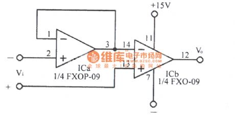
Zero-drift operational amplifier circuit diagram as shown:
(View)
View full Circuit Diagram | Comments | Reading(1663)
Zero drift inverting amplifier circuit diagrams
Published:2014/3/20 21:05:00 Author:lynne | Keyword: Zero drift inverting amplifier circuit diagrams,
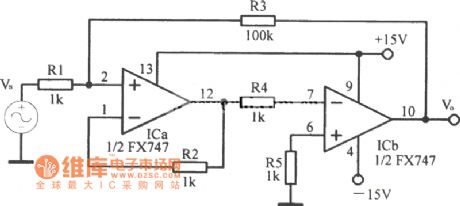
Zero drift inverting amplifier circuit diagrams shown as following:
(View)
View full Circuit Diagram | Comments | Reading(1534)
The output voltage of the op amp circuit diagram
Published:2014/3/19 21:15:00 Author:lynne | Keyword: The output voltage of the op amp circuit diagram,
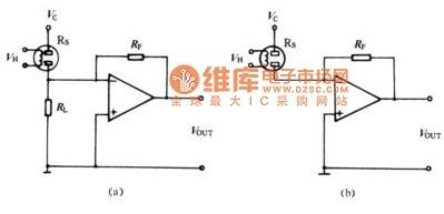


The output voltage of the op amp circuit diagram shown as follow:
(View)
View full Circuit Diagram | Comments | Reading(1418)
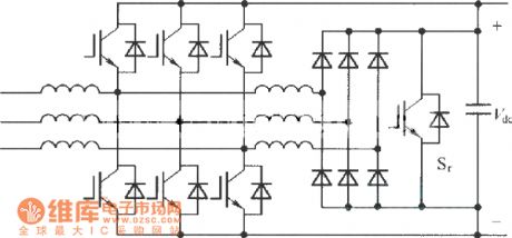
ZVT three-phase Boost rectifier input circuit diagram
Published:2014/2/17 21:36:00 Author: | Keyword: ZVT three-phase Boost rectifier input circuit diagram,
View full Circuit Diagram | Comments | Reading(1167)
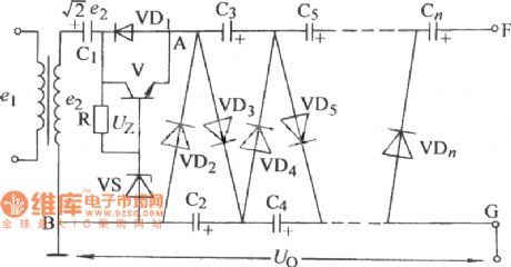
The output voltage adjustable voltage type multiple rectifier circuit diagram
Published:2014/2/16 21:32:00 Author: | Keyword: The output voltage adjustable voltage type multiple rectifier circuit diagram,
View full Circuit Diagram | Comments | Reading(1228)
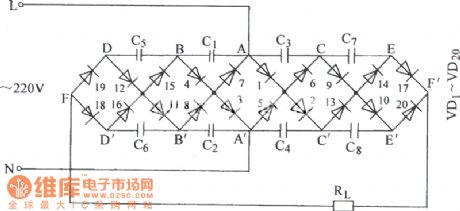
Covering series high voltage rectifier bridge circuit diagram
Published:2014/2/16 21:31:00 Author: | Keyword: Covering series high voltage rectifier bridge circuit diagram,
View full Circuit Diagram | Comments | Reading(1441)
RS232 circuit
Published:2014/2/9 20:53:00 Author:lynne | Keyword: RS232 circuit, RS232
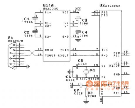
RS232 circuit shown in Figure:
(View)
View full Circuit Diagram | Comments | Reading(1225)
RS232 RS485 interface schematic diagram
Published:2014/2/7 19:49:00 Author:lynne | Keyword: RS232 RS485 interface schematic diagram, RS232, RS485
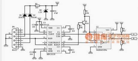
RS232 RS485 interface schematic diagram as shown in Figure:
(View)
View full Circuit Diagram | Comments | Reading(3870)
A circuit diagram with hysteresis characteristics
Published:2014/2/6 20:40:00 Author: | Keyword: A circuit diagram with hysteresis characteristics,
A circuit diagram with hysteresis characteristics
(View)
View full Circuit Diagram | Comments | Reading(968)
LED flow display clocks hardware circuit diagram
Published:2014/1/15 18:29:00 Author: | Keyword: LED flow display clocks hardware circuit diagram,
LED flow display clocks hardware circuit diagram
(View)
View full Circuit Diagram | Comments | Reading(1666)
Article 20 the beam of light line display device driver circuit diagram
Published:2014/1/14 18:22:00 Author: | Keyword: Article 20 the beam of light line display device driver circuit diagram,
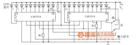
Article 20 the beam of light line display device driver circuit diagram
(View)
View full Circuit Diagram | Comments | Reading(983)
IC card read/write circuit diagram
Published:2014/1/5 19:56:00 Author:lynne | Keyword: IC card read/write circuit diagram,
IC card read/write circuit diagram as shown: (View)
View full Circuit Diagram | Comments | Reading(1109)
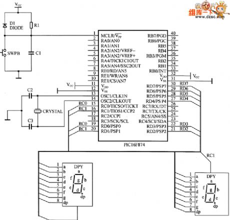
PIC16F877 and interface of MG-12232 module circuit diagram
Published:2014/1/5 19:53:00 Author:lynne | Keyword: PIC16F877 and interface of MG-12232 module circuit diagram, PIC16F877
PIC16F877 and interface of MG-12232 module circuit diagramis shown in Fig.:
(View)
View full Circuit Diagram | Comments | Reading(1129)
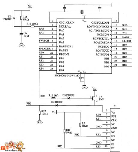
PIC16F887 hardware circuit diagram
Published:2014/1/2 20:07:00 Author:lynne | Keyword: PIC16F887 hardware circuit diagram, PIC16F887
PIC16F887 hardware circuit diagram as shown:
(View)
View full Circuit Diagram | Comments | Reading(2296)
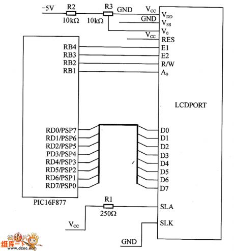
LCD and the interface of PIC16F877 circuit
Published:2014/1/2 20:09:00 Author:lynne | Keyword: LCD and the interface of PIC16F877 circuit, PIC16F877
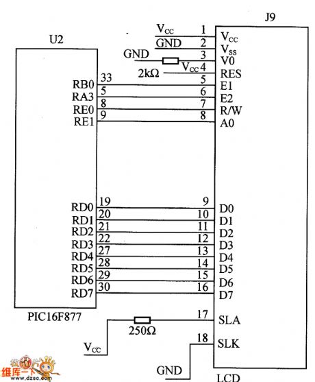
LCD and the interface of PIC16F877 circuit shown in Fig.:
(View)
View full Circuit Diagram | Comments | Reading(962)
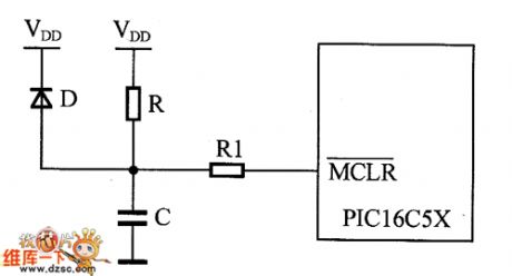
Button Reset circuit diagram
Published:2014/1/1 20:41:00 Author:lynne | Keyword: Button Reset circuit diagram,
Button Reset circuit diagram shown in Figure:
(View)
View full Circuit Diagram | Comments | Reading(1109)
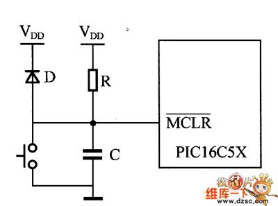
External power-on reset circuit
Published:2014/1/1 20:40:00 Author:lynne | Keyword: External power-on reset circuit,
External power-on reset circuit shown in Figure: (View)
View full Circuit Diagram | Comments | Reading(2207)
| Pages:3/250 1234567891011121314151617181920Under 20 |
Circuit Categories
power supply circuit
Amplifier Circuit
Basic Circuit
LED and Light Circuit
Sensor Circuit
Signal Processing
Electrical Equipment Circuit
Control Circuit
Remote Control Circuit
A/D-D/A Converter Circuit
Audio Circuit
Measuring and Test Circuit
Communication Circuit
Computer-Related Circuit
555 Circuit
Automotive Circuit
Repairing Circuit