
Amplifier Circuit
Index 5
TDA2003 Audio Amplifier Circuits
Published:2013/10/9 19:53:00 Author:lynne | Keyword: TDA2003 Audio Amplifier Circuits
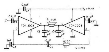
TDA2003 is a cheap amplifier that is designed to run on single rail power supplies (unipolar). It provides a high output current capability (up to 3.5A), very low harmonic and cross-over distortion.TDA2003 10W car radio audio amplifier
TDA2003 18W bridged audio amplifier
TDA2003 can be used as an BCL (bridged amplifier) and car deliver up to 18W.
(View)
View full Circuit Diagram | Comments | Reading(2524)
TDA2005 Audio Amplifier Circuits
Published:2013/10/8 20:17:00 Author:lynne | Keyword: TDA2005 Audio Amplifier Circuits
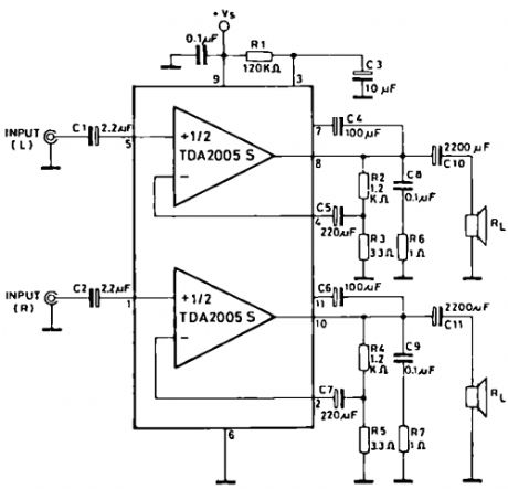
TDA2005 is a class B dual audio power amplifier specifically designed for car radio applications. Its high current capability (up to 3.5 A) and the ability to drive very low impedance loads (down to 1.6 ohms) makes this circuit a good choice for cheap power booster amplifiers. (View)
View full Circuit Diagram | Comments | Reading(1670)
TDA2030 Audio Amplifier Circuits
Published:2013/10/8 20:16:00 Author:lynne | Keyword: TDA2030 Audio Amplifier Circuits
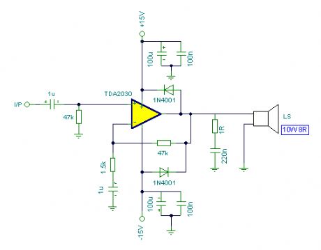
TDA2030 is a monolithic integrated circuit in Pentawatt package, intended for use as a low frequency class AB amplifier. It provides 14W output power (d = 0.5%) at 14V/4Ω at ± 14V or 28V, the guaranteed output power is 12W on a 4Ω load or 8W on a 8Ω
TDA2030 10W audio amplifier circuit
TDA 2030 audio amplifier can output 20 W but in this schematic we have reduced the power to 10W and we use 10w speakers.
(View)
View full Circuit Diagram | Comments | Reading(1778)
TDA7294 Audio Amplifier Circuits
Published:2013/10/8 20:14:00 Author:lynne | Keyword: TDA7294 Audio Amplifier Circuits
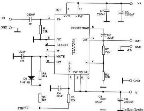
TDA7294 is a monolithic integrated circuit in Multiwatt15 package, with high output power (up to 100W) intended for use as audio class AB amplifier in Hi-Fi field applications (Home Stereo, self powered loudspeakers, Topclass TV). Thanks to the wide voltage range and to the high out current capability it is able to supply the highest power into both 4W and 8W loads even in presence of poor supply regulation, with high Supply Voltage Rejection. (View)
View full Circuit Diagram | Comments | Reading(1892)
AC Power Monitor IC
Published:2013/9/21 21:11:00 Author:lynne | Keyword: AC Power Monitor IC
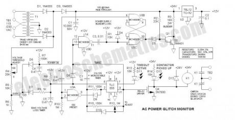
This AC Power Monitor continuously watches the AC power line voltage for both under-voltage and missing cycles. When it detects a total of 5 or 6 consecutive missing half-cycles (50mS, 50/60HZ), it drops a relay and starts a timer. A power contactor is slaved to the relay contacts. Its purpose is to protect power-loss sensitive industrial equipment from brief power glitches by preventing immediate restart.
After the specified time delay (2 to 10S), the equipment may automatically restart. Although this may seem like a simple task, note that the condition sensed is the absence of a periodic signal and that the timer may or may not have external power available. electroschematics.com is not really into industrial controls, but this may be the beginning—this is where I spent most of my life.
This function could also be performed by a PLC (programmable logic controller) with a UPS (unterruptable power source), but such would be expensive and consume additional panel space.
Two key components (transformer and relay) are documented on the power monitor schematic — there is no bill of materials.
Power supply
Key to this functioning properly is its power-loss ride-through capability. Note that this circuit continues to time out even after the power is interrupted. To run the circuitry for the entire time period, energy is stored in a large filter capacitor (10,000uf). That way if the power resumes during the timeout period, the timer remains alive and functioning so that the sensitive equipment may not restart.The raw capacitor voltage ranges from about 14 to 24V, and is series regulated to 12V via U2, an LM7812 voltage regulator.
The power transformer (T1) provides low voltage power and power line isolation. Its primary is reconnectable for 115 /230VAC.
Capacitor Bleeder
At the end of the timeout period, the bleeder circuit kicks in to dump the remaining charge. A 4000 series CMOS latch consisting of U3B & U3C is set by the positive transition of U1-3. Should the power resume while the capacitor is bleeding down, the latch is reset via the signal at the collector of Q3 so that the bleeder driver Darlington (Q1 & Q2) turns off. When all of the charge is dissipated by the bleeder resistor (R3), the circuit is free to immediately restart and again monitor voltage glitches.
The MC14093 is a good choice for the power monitor application. It has Schmitt trigger inputs for handling slow input signal transitions, and may be powered by the 12V Vcc. It is identical in pin-out to the more common CD4011. Note that the CD4011 should also function acceptably, but I did not try it in the circuit.
Timer
The timer is the good old 555 (actually, it is the TLC555 due to its low quiescent current). It is configured as a monostable multivibrator that is triggered via a positive voltage at U1-6. To assure that the internal latch of the 555 is set in the proper state during power-up, C7 works against Vcc (rather than common) and U1-2 is held low for 0.5 sec via U3A, C6 and R10.
The timeout period may be increased substantially by increasing the size of the timing capacitor C7. Note that C1 must be adjusted likewise to provide additional ride-through. 60 seconds is not unreasonable.
AC voltage threshold detector
Note that the cathodes of D1 & D2 are unfiltered—this is necessary for rapid sensing of power loss—a filter capacitor would tend to hold up the voltage thus interfering with the voltage loss timer. The filter capacitor (C1) is isolated via D3. The Vbe of Q3 (0.65V) is the voltage threshold comparator. This voltage is multiplied by the ratio of (R4, R5 & R6) to R6.
The function of the voltage threshold comparator is to keep C5 discharged. At each line voltage zero-crossing C5 charges slightly, but requires a full 50mS to reach the threshold of U1-6. Should the voltage remain below the threshold of Q3, C5 starts to charge significantly—if 5 or 6 half-cycles are lost in succession, the voltage across C5 charges to the 8V threshold of U1-6 and triggers the timer.
Proper adjustment of R4 is required. To do so, connect a Variac to the power terminals and reduce the voltage to the desired AC threshold voltage (e.g. 170VAC). Then increase the value of R16 until the LEDs change state. (View)
View full Circuit Diagram | Comments | Reading(1645)
70 Watt MOSFET Audio Amplifier
Published:2013/8/27 2:26:00 Author:lynne | Keyword: 70 Watt MOSFET Audio Amplifier
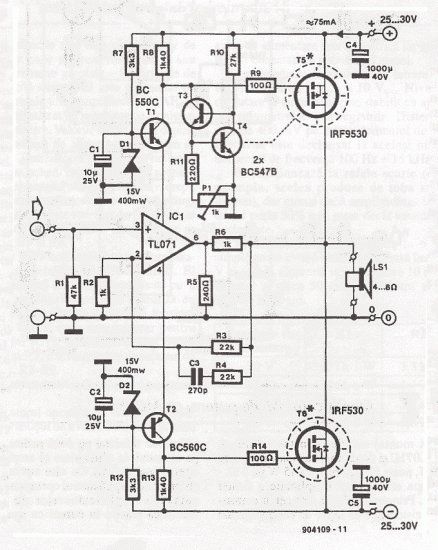
This simple power mosfet audio amplifier circuit, with TL071C and 2 MOSFETs (IRF9530 and IRF530) can deliver up to 45 Watts on 8 Ω speaker. This schematic is based on Siliconix application and on variations of voltage on the 2 resistors that are serial inserted on the voltage supplier of the operational amplifier driver. The MosFet transistor must be mounted on a heatsink with at least 1K/W.
Amplifier’s efficiency is 70%, distortions at cut frequency were at most 0.2% at 20Hz on 8 Ω and 10W. With a power supply of ± 30V the mosfet audio amplifier can deliver 45W on 8 Ω and 70w on 4 Ω. Remember that this audio amplifier is not protected on shortcircuits so everytime you switch on check to see if the speaker is connected.
(View)
View full Circuit Diagram | Comments | Reading(2222)
TDA2030 10W Audio Amplifier Circuit
Published:2013/8/27 2:21:00 Author:lynne | Keyword: TDA2030 10W Audio Amplifier Circuit

TDA2030 audio amplifier can output 20 W but in this schematic we have reduced the power to 10 Watts and we use 10 W speakers. The input sensivity is around 200 mV and the amplifier is set by the 47 k and 1.5 k resistors.
(View)
View full Circuit Diagram | Comments | Reading(1482)
Low Voltage Audio Amplifier
Published:2013/8/26 1:12:00 Author:lynne | Keyword: Low Voltage Audio Amplifier
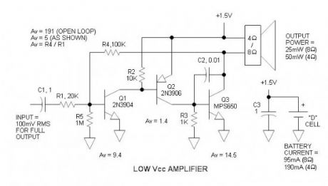
This experimental (3) transistor class A audio power amplifier delivers 25mW into an 8Ω load, or 50mW into a 4Ω load using only a 1.5V power source. At such low voltages, there are many issues to consider and much to learn. To the best of my knowledge the following information is new to the world.
Background
Months ago, I indicated an intention to write a piece on low voltage transistor application for another of my Single Transistor Amplifier Revisited series. Then a few weeks ago, Daniela, who participates in our forum, asked the simple, but profound question: “what is the minimum operating voltage of a transistor?” While, Mr. Marian attempted to narrow the scope of the question, no answers were given. This is on the heels of a similar article concerning Low Voltage Operation of the 555.
Theoretical minimum vs. practical minimum voltage
For a silicon bipolar transistor, the initial voltage requirement is to exceed the Vbe junction voltage of 0.6V. Then, to be able to current regulate this voltage via a series resistor, the source voltage must be about double this or about 1.2V. (The rule of thumb for shunt voltage regulators is that the source voltage is recommended to be double the regulated voltage.) This is perhaps the theoretical minimum Vcc. The practical minimum takes into consideration low voltage power sources – in this case, the ubiquitous 1.5V single cell battery is perhaps the standard low voltage power source – this is the power source for my circuit.
(View)
View full Circuit Diagram | Comments | Reading(1844)
LA4440 Audio Amplifier
Published:2013/8/13 3:58:00 Author:lynne | Keyword: LA4440 Audio Amplifier
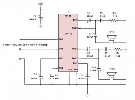
A simple audio amplifier based on the LA4440 IC. This will take your computer’s headphone level output and amplify it to drive a pair of external speakers. If you are listening to music or movies on laptops and computers, this is a useful little project for you. Laptop speakers are never loud enough to give satisfying listening. They give users the ability to hear something, but for anything like music or movie soundtracks they are very poor performers. The output from a laptops built in speakers is just too low, and this circuit addresses that low power with some additional amplification.
This circuit uses an LA4440 and some supporting components to give you much more power, while retaining a small package that you can use. The IC is a dual channel audio power amplifier, with low distortion, and a good frequency range.
Using 2 channels, the LA4440 will output 6 watts per channel, that can drive much larger speakers than a laptop can hold. When you set up a small enclosure(s), a 12V power supply, and an audio jack connection to the laptop you’ll have a nice enhancement to your laptop audio enjoyment.
(View)
View full Circuit Diagram | Comments | Reading(2321)
Single Transistor Amplifier Revisited – Part 4
Published:2013/8/8 20:20:00 Author:lynne | Keyword: Single Transistor Amplifier Revisited, Part 4
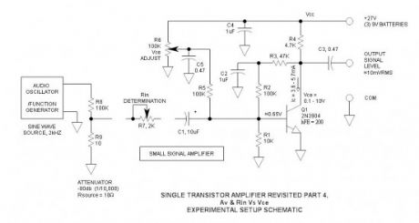
What happens to voltage gain when a bipolar transistor is operated at low voltages (Vce < 1V). In a previous circuit that operated at a quiescent Vce of 0.75V, voltage gain was demonstrably low. This experiment is an attempt to quantify what actually happens to voltage gain and input resistance in a general purpose transistor over the range of Vce = 0.1 to 10V. The results are interesting and informative.
(View)
View full Circuit Diagram | Comments | Reading(1590)
Linear FM 50Watt with BLY90
Published:2013/7/22 20:03:00 Author:muriel | Keyword: Linear , FM, 50Watt, BLY90
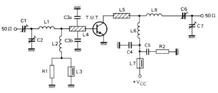
A amplifier of force RF for the FM, is always essential for the amateur that wants it strengthens some small transmitter, that likely already it has manufactured or has been supplied ready. The present circuit can give 50-60W RF force of expense, with control smaller than 15-20W in the region of frequencies of FM, that is to say in the 88-108MHZ. Transistor that we selected for this manufacture is the BLY90, that has gain 5dB.
As it appears in the analytic drawing (image 1) the amplifier is manufactured with transistor TR1, type BLY90 of Philips. The transistor this is specifically drawn for operation in frequencies up to 175MHZ, with very good results of linearity and record of force. In his technical' characteristics they are included the tendency of operation in the 12V the current of collector in the gain expense in the 5dB (measured in order C) and force of entry in the 16W. Variable capacitors C1, C2, with inductor L1, constitute the circuit of co-ordination, that adapts the exit of our transmitter in amplifier RF. This circuit has been calculated suitably, so that it covers all band the FM with the biggest possible output.Inductor RFC1 polarized the transistor, so as to it works in order C, that is to say with the biggest output. Inductor L2 in the collector of TR1, constitutes the charge of amplifier, while RFC2 prevents the RF signals leak in the line of catering. Capacitor C2 and resistance R1, protect the circuit from auto polarization. The coordinated circuit of expense that is constituted by inductor L2 and variable capacitors C3, C4, adapts the exit of amplifier RF with the next stage, which can be constituted from some amplifier RF of high force (> 300W) or a aerial. This circuit can be supplied with 12V f.e from the battery of one automotive, so that it renders the system emitter portable. Thus, easily it can be moved in points with bigger altitude, in order that from there are achieved radio transmissions, something that was also got used in the past by romantic amateur of radio band. The manufactureThe manufacture of amplifier, is very simple and easy, it is enough to look the images 3 and 2 that portray pcb the amplifier and the placement of materials in this. Puncture the point pcb, that pass the nutshell of TR1. Sticks the capacitors, variable, the resistance, RF tsok and the inductors. Finally you stick TR1, being careful not overheating at the welding and bend the pins his. Clean finally pcb from the residues of iron. Make a very careful control for by any chance errors, omissions, short-circuits, chills you stick also anything other that could you make think that will not work the amplifier.
If all they are it includes, you connect the exit of your transmitter (15-20W) in input the amplifier. The exit of amplifier him you will connect in some charge (dummy load) or in the aerial, through bridge stagnant waves. Supply with tendency 11-15V your amplifier (power supply it should gives current 4-5A). Regulate the 4 variable C1-C4, until you take the biggest force of expense. The amplifier is ready.
Note:TR1 needs a wiper of dimensions 5x10cm for trouble free operation. This wiper in TR1, without insulator, after his central screw has electric isolation from remainder pins.
PartsC1-C4 = 10-80pF C5 = 10nF C6 = 1000pF C7 = 100nF C8 = 2200mF/35V L1 = 1 coils of diameter of 10mms, 1mmL2 = 7 coils of diameter of 10mms, 0,8mmsL3 = 3 coils of diameter of 10mms, 1mmTR1 = BLY90 (View)
View full Circuit Diagram | Comments | Reading(1122)
20dB VHF Amplifier
Published:2013/7/22 19:57:00 Author:muriel | Keyword: 20dB , VHF Amplifier
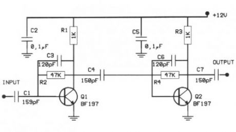
Many times we needed to strengthen a small signal in the region of VHF or FM, or it is we lead a body, or a receptor. The preamplifier that to you we propose offers 20dB in all the region of VHF and it still can reach also their 500MHZ. The amplifier is a circuit of high frequency RF with distinguishable materials. The amplifier as circuit strengthens the tendency of signal with concrete aid, depending on the frequency of signal. If the frequency of signal is included in the limits of spectrum of frequencies of amplifier, then it is strengthened, otherwise it is downgraded. Each amplifier of this category, accordingly with his designing, strengthens a concrete region of frequencies and obeys in same characteristics. The one that to you we present today concerns the regions of VHF where they exist and the corresponding television stations for channels 5 until 12. His circuit he is enough simple, so that it is made easily with materials that exist in the trade. It is based on transistors with aid until the 500MHZ. The type of transistor can be BF197 or some other.
In form 1 appears the theoretical circuit of amplifier. As we see it is constituted from two similar circuits (rungs). In this circuits are not included in joint action circuits. With that way is covered a wide spectrum of frequencies, without is differentiated abruptly the aid as for the frequency. With this provision we have smaller gain but big breadth of frequencies. The two rungs are same, with the same prices of materials and each rung offer aid roughly 10dB. The transistors and the remainder materials, because the industrial manufacture, have almost the same characteristics. Associates the particular characteristics of demagogues are altered mainly the aid of rung. Each rung uses a transistor of type npn in provision of common emitter that functions in order A. his rungs works in provision of common emitter with null resistance in emitter. In each rung a network of resistances between the collectors and the bases polarize the transistors and ensures the operation of circuit. The junction between the rungs becomes via ceramic capacitors of small capacity from 0,1nF until 0,22nF (at preference ceramic). In the place of two rungs we can try various transistors of independent company or even different between them. The circuit of course cannot work with all of them. The tendency of catering should emanate from stabilised power supply with tendency 12V. Depending on the tendency of catering and the type of transistor, in each rung of amplifier it needs enter also different resistances. Force of expense, under conditions of high excitation it can exceed the 1 mW
Manufacture The total aid of circuit, according to the elements of transistors, reaches 20dB. Enough aid for a lot of applications. The amplifier is drawn in order to it has big response of frequency up to 0,5Ghz. According to the particular characteristics of manufacture, the better application that we could to you propose for this designing would be the aid of television signal emanating from a small transmitter of television or the preamplifier of a frequency meter. The assembly of amplifier is realised above in printing form 2. In this you will place all the materials according to form 3. The manufacture, in order to it works right it needs one small stabilised power supply 12V. The consumption of circuit is small hardly some mA. The resistance en line with the collector is 10 000. When you finish the construction and the control of manufacture, place the PCB in metal box of suitable dimensions. PartsR1 1KC3 120pFR2 47KC4 150pFR3 1KC5 0,1uFR4 47KC6 120pFC1 150pFC7 150pFC2 0,1uFQ1 Q2 BF197 (View)
View full Circuit Diagram | Comments | Reading(1584)
60W Linear amplifier
Published:2013/7/21 20:36:00 Author:muriel | Keyword: 60W , Linear amplifier
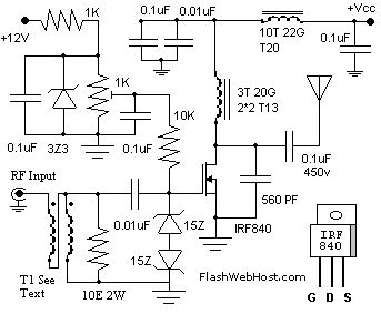
The 60 Watt linear amplifier is simple all solid state circuit using power mosfet IRF840. The IRF series of power transistors are available in various voltage and power ratings. A single IRF840 can handle maximum power output of 125 watts. Since these transistors are used in inverters and smps they are easily available for around Rs: 20/-.
The IRF linear amplifier can be connected to the out put of popular VWN-QRP to get an output of 60 Watts. The circuit draws 700 ma at 60 Volt Vcc. Good heat sink is a must for the power transistor.
Alignment of the circuit is very easy. Connect a dummy load to the out put of the circuit. You can use some small bulb like 24V 6Watts as the dummy load. I have even used 230V 60Watts bulb as dummy load with my IRF840 power amplifier working at 120Volts. Adjust the 10K preset to get around 100 ma Drain current. I used gate voltage of 0.8V with my linear amplifier. A heigh gate voltage can make the power transistor get distroyed by self oscillation. So gate voltage must be below 2V and fixing at 1V will be safe.
Bifalar transformaer T1 is wound with 8 turns 26SWG on 1.4 x 1 balun core.The coil on the drain of IRF is 3 turns 20 SWG wound on 4 number of T13.9 torroids (two torroids are stacked to form a balun core). The RFC at the Vcc line is 20 Turns 20 SWG wound on T20 torroid.
(View)
View full Circuit Diagram | Comments | Reading(1293)
Muscular Bio-Stimulators
Published:2013/7/17 21:37:00 Author:muriel | Keyword: Muscular Bio-Stimulators
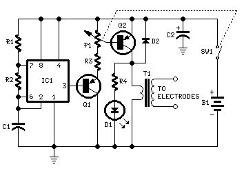
Parts:P1 4K7 Linear PotentiometerR1 180K 1/4W ResistorR2 1K8 1/4W Resistor (see Notes)R3 2K2 1/4W ResistorR4 100R 1/4W ResistorC1 100nF 63V Polyester CapacitorC2 100µF 25V Electrolytic CapacitorD1 LED Red 5mm.D2 1N4007 1000V 1A DiodeQ1,Q2 BC327 45V 800mA PNP TransistorsIC1 7555 or TS555CN CMos Timer ICT1 220V Primary, 12V Secondary 1.2VA Mains transformer (see Notes)SW1 SPST Switch (Ganged with P1)B1 3V Battery (two 1.5V AA or AAA cells in series etc.)
Device purpose:This is a small, portable set, designed for those aiming at look improvement. The Bio-Stimulator provides muscles' stimulation and invigoration but, mainly, it's an aid in removing cellulitis.Tape the electrodes to the skin at both ends of the chosen muscle and rotate P1 knob slowly until a light itch sensation is perceived. Each session should last about 30 - 40 minutes.
Circuit operation:IC1 generates 150µSec. pulses at about 80Hz frequency. Q1 acts as a buffer and Q2 inverts the pulses' polarity and drives the Transformer. Output pulses' amplitude is set by P1 and approximately displayed by LED D1 brightness. D2 protects Q2 against high voltage peaks generated by T1 inductance during switching.
Notes:T1 is a small mains transformer 220 to 12V @ 100 or 150mA. It must be reverse connected i.e.: the 12V secondary winding to Q2 Collector and ground, and the 220V primary winding to output electrodes.Output voltage is about 60V positive and 150V negative but output current is so small that there is no electric-shock danger.In any case P1 should be operated by the patient , starting with the knob fully counter-clockwise, then rotating it slowly clockwise until the LED starts to illuminate. Stop rotating the knob when a light itch sensation is perceived.Best knob position is usually near the center of its range.In some cases a greater pulse duration can be more effective in cellulitis treatment. Try changing R2 to 5K6 or 10K maximum: stronger pulses will be easily perceived and the LED will shine more brightly.Electrodes can be obtained by small metal plates connected to the circuit's output via usual electric wire and can be taped to the skin. In some cases, moistening them with little water has proven useful.SW1 should be ganged to P1 to avoid abrupt voltage peaks on the patient's body at switch-on, but a stand alone SPST switch works quite well, provided you remember to set P1 knob fully counter-clockwise at switch-on.Current drawing of this circuit is about 1mA @ 3V DC.Some commercial sets have four, six or eight output electrodes. To obtain this you can retain the part of the circuit comprising IC1, R1, R2, C1, C2, SW1 and B1. Other parts in the diagram (i.e. P1, R3, R4, D1, D2, Q2 & T1) can be doubled, trebled or quadrupled. Added potentiometers and R3 series resistors must be wired in parallel and all connected from Emitter of Q1 to positive supply.Commercial sets have frequently a built-in 30 minutes timer. For this purpose you can use the Timed Beeper the Bedside Lamp Timer or the Jogging Timer circuits available in this Website, adjusting the timing components to suit your needs.
(View)
View full Circuit Diagram | Comments | Reading(1269)
Amplifier of acoustic frequencies with preamplifier
Published:2013/7/15 20:22:00 Author:muriel | Keyword: Amplifier , acoustic frequencies, preamplifier
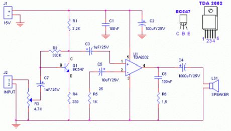
Technical characteristics:Tendency of catering: 15VForce of expense: 4,2Wrms in the 4WMinimal signal of entry: 94mVp-p with preamplifier, 0,65Vp-p without the preamplifier.
Parts:R1 2,2KWR2 330KWR3 4,7KW logarithmic potentiometerR4 330WR5 1KWR6 1,5WC1, C6 100nF polyesterC2 100mF/25V ilektrolytjko'sC3, C7 1mF/25V electrolyticC4 1000uF/25V electrolyticC5 10uF/25V electrolyticQ1 BC547U1 TDA2002LS1 Loudspeaker.
Notes:Proportionally the resistance of loudspeaker changes the force that it can give the amplifier:LS1 Force of expense2W 6,5Wrms4W 4,2Wrms6W 3Wrms8W 2,25Wrms
(View)
View full Circuit Diagram | Comments | Reading(1354)
Low impedance microphone amplifier
Published:2013/7/15 20:15:00 Author:muriel | Keyword: Low impedance, microphone amplifier
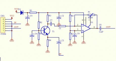
The circuit is a microphone amplifier for use with low impedance (~200 ohm) microphones. It will work with stabilized voltages between 6-30VDC. If you don't build the impedance adapter part with T1, you get a micamp for higher impedance microphones. In this case, you should directly connect the signal to C7.
(View)
View full Circuit Diagram | Comments | Reading(1064)
Guitar Amplifiers
Published:2013/7/15 20:14:00 Author:muriel | Keyword: Guitar Amplifiers
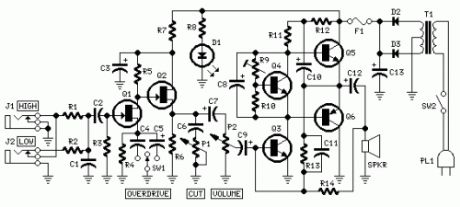
View full Circuit Diagram | Comments | Reading(1233)
Motorola Hi-Fi power amplifier
Published:2013/7/15 20:13:00 Author:muriel | Keyword: Motorola , Hi-Fi, power amplifier

This is a very simple, low cost, Hi-Fi quality power amplifier. You can build it 5 ways, like it’s shown in the table (from 20 W to 80 W RMS).
Some comments:- The first thing that you must do, is to measure the end transistors (T3 and T4) amplifying coefficient, the hfe or β. If their disagreement is bigger than 30 %, the amplifier would not give a clear sound. I used MJ3001 and MJ2501 transistors, and this disagreement was around 5%.- Before the first “turning on†you must short circuit the inputs of the amp, and put a mA-meter on the output, than turn the amplifier on, and tune the R13 pot, to decrease the DC current on the output, to some uA-s, or in a lucky situation to zero. I was able to decrease it to 10 uA.
(View)
View full Circuit Diagram | Comments | Reading(1777)
10W Audio Amplifier
Published:2013/7/15 20:04:00 Author:muriel | Keyword: 10W , Audio Amplifier
Parts:P1 22K Log.Potentiometer (Dual-gang for stereo)P2 100K Log.Potentiometer (Dual-gang for stereo)R1 820R 1/4W ResistorR2,R4,R8 4K7 1/4W ResistorsR3 500R 1/2W Trimmer CermetR5 82K 1/4W ResistorR6,R7 47K 1/4W ResistorsR9 10R 1/2W ResistorR10 R22 4W Resistor (wirewound)C1,C8 470nF 63V Polyester CapacitorC2,C5 100uF 25V Electrolytic CapacitorsC3,C4 470uF 25V Electrolytic CapacitorsC6 47pF 63V Ceramic or Polystyrene CapacitorC7 10nF 63V Polyester CapacitorC9 100nF 63V Polyester CapacitorD1 1N4148 75V 150mA DiodeIC1 NE5532 Low noise Dual Op-ampQ1 BC547B 45V 100mA NPN TransistorQ2 BC557B 45V 100mA PNP TransistorQ3 TIP42A 60V 6A PNP TransistorQ4 TIP41A 60V 6A NPN TransistorJ1 RCA audio input socket
Power supply parts:R11 1K5 1/4W ResistorC10,C11 4700uF 25V Electrolytic CapacitorsD2 100V 4A Diode bridgeD3 5mm. Red LEDT1 220V Primary, 12 + 12V Secondary 24-30VA Mains transformerPL1 Male Mains plugSW1 SPST Mains switch
This design is based on the 18 Watt Audio Amplifier, and was developed mainly to satisfy the requests of correspondents unable to locate the TLE2141C chip. It uses the widespread NE5532 Dual IC but, obviously, its power output will be comprised in the 9.5 - 11.5W range, as the supply rails cannot exceed ±18V.As amplifiers of this kind are frequently used to drive small loudspeaker cabinets, the bass frequency range is rather sacrificed. Therefore a bass-boost control was inserted in the feedback loop of the amplifier, in order to overcome this problem without quality losses. The bass lift curve can reach a maximum of +16.4dB @ 50Hz. In any case, even when the bass control is rotated fully counterclockwise, the amplifier frequency response shows a gentle raising curve: +0.8dB @ 400Hz, +4.7dB @ 100Hz and +6dB @ 50Hz (referred to 1KHz).
Notes:Can be directly connected to CD players, tuners and tape recorders.Schematic shows left channel only, but C3, C4, IC1 and the power supply are common to both channels.Numbers in parentheses show IC1 right channel pin connections.A log type for P2 ensures a more linear regulation of bass-boost.Don't exceed 18 + 18V supply.Q3 and Q4 must be mounted on heatsink.D1 must be in thermal contact with Q1.Quiescent current (best measured with an Avo-meter in series with Q3 Emitter) is not critical.Set the volume control to the minimum and R3 to its minimum resistance.Power-on the circuit and adjust R3 to read a current drawing of about 20 to 25mA.Wait about 15 minutes, watch if the current is varying and readjust if necessary.A correct grounding is very important to eliminate hum and ground loops. Connect in the same point the ground sides of J1, P1, C2, C3 &C4. Connect C9 at the output ground.Then connect separately the input and output grounds at the power supply ground.
Technical data:Output power: 10 Watt RMS @ 8 Ohm (1KHz sinewave)Sensitivity: 115 to 180mV input for 10W output (depending on P2 control position)Frequency response: See Comments aboveTotal harmonic distortion @ 1KHz: 0.1W 0.009% 1W 0.004% 10W 0.005%Total harmonic distortion @ 100Hz: 0.1W 0.009% 1W 0.007% 10W 0.012%Total harmonic distortion @10KHz: 0.1W 0.056% 1W 0.01% 10W 0.018%Total harmonic distortion @ 100Hz and full boost: 1W 0.015% 10W 0.03%Max. bass-boost referred to 1KHz: 400Hz = +5dB; 200Hz = +7.3dB; 100Hz = +12dB; 50Hz = +16.4dB; 30Hz = +13.3dB
(View)
View full Circuit Diagram | Comments | Reading(1363)
Speaker Box Audio Amp
Published:2013/7/15 20:03:00 Author:muriel | Keyword: Speaker Box, Audio Amp
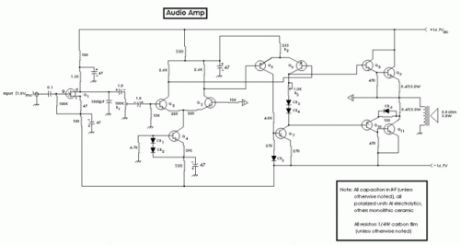
I did this design after getting a new computer. After buying the processor, monitor, and printer, I wasn't willing to spring for a set of speakers too. After going soundless , I decided to add speakers. Of course, this was the perfect excuse warm up the soldering iron to try out a new design. This original design is a variation on a well-known design, examples of which can be found in a great many texts. My variation was to add a second differential stage to replace the usual common emitter-plus-constant current source. Doing so opens up a second inverse feedback path. The signal path being a series connection of the differential amp inverting inputs, and the feedback being the non-inverting inputs. To this end, the constant current source does not include bypass capacitors to render it a DC-only stage. The other feedback path is the usual one: output to the non-inverting input of the first differential stage. The idea is to add lots of inverse feedback in order to linearize the output transistors, as the non-linearity of these devices makes them rather poor analog amplifiers.
The other design criterion was the use of components readily available at a hobbist's store: Radio Shack . No exotic components that would require a special order are used here. To this end, the output stage is a semi-complementary design, although this is not optimum so far as fidelity is concerned. (Radio Shack doesn't offer complimentary pairs of power BJTs.) Since the amp is intended to work into the wide band (60Hz -- 18KHz) speakers that this store sells, the gain is deliberately kept down. With the design given here, the max output is 6.0W. Even here, since these speakers are rated at 3.0W, you could blow speakers if the volume is turned up too high. Limiting output is accomplished with the initial voltage amp (Q1). This stage has a gain of 7.5, so that with a 1.0VRMS input, the output voltage becomes slightly less than 7.5VRMS. The gain of the circuit from the output end of the volume control to the speaker is unity, due to the large negative feedback. You could drive the power output as high as 10W, as there is plenty of head room in the power supply design. (Again, this was done to improve the fidelity as much as possible with a BJT-based design.) If you push the output, you will need better heat sinking on the finals than what's described here.The selection of actual components is not critical. Any small signal transistors anonymous will work here. The only exception is Q8 and Q10. These two must be a 2N3904 and a 2N3906, as these are complimentary pairs. These transistors set the characteristics for the entire final, and must be balanced as to characteristics in order to keep DC out of the speakers, and for symmetrical amplification. As for the differential pairs (Q2, Q3, Q5, Q6) type isn't so important, however, matched pairs is important. It's a good idea to get a couple dozen of each, PNP and NPN, and select pairs that match closely in VBE and hFE. Matching pairs in the differential stages helps hold down DC offset, as this design uses DC coupling in the interest of good low frequency response. Speakers tend to object to any significant amount of DC by burning out the voice coils. It also compromises fidelity in that DC on the voice coils restricts the movement of the cone.The 1800pF capacitor connected to the drain of Q1 was included since one of these amps showed a weak (10mVP-P) oscillation at 700KHz. If you include it, be certain to make the connection with the least possible lead length, as it is an RF component. It will have no effect on the audio quality since its cutoff frequency is about 58KHz.
Construction: AmplifierThe entire unit is designed to fit in a plastic project box cabinet of 7 X 6 X 3 inches. The wide band speakers are 3¾ inches in diameter, and fit in a cutout of 37/16 inches. The circuit board is: 6¾ X 2¼ double-sided, copper clad. The circuit is built dead bug style, simply by making all ground connections by soldering to the unetched copper, the rest of the wiring being made above the circuit board. If additional mechanical reinforcement is needed, this is provided by soldering 2.2MEG resistors to the copper ground plane for use as a tie point . Connecting such large resistors between the circuit and ground doesn't affect the operation since the impedance at that point is going to be several orders in magnitude smaller. To fit the circuit on the board, both sides are used. The preamp module being constructed on one side, with the final being built on the opposite side.The heat sink for the power transistors is made from two pieces of steel or aluminum 1 X 1 (in.) angle stock. Simply measure off a 2¼ length, and cut it in half. This will naturally provide the necesary gap to separate these heat sinks electrically. Sand off enough copper from one end of the circuit board to insure that the heat sinks aren't being shorted out. These are attached to the circuit board with one screw and nut. (Also, be sure to clear the copper away from the screw heads on the preamp side of the circuit board, otherwise, you will short out the finals.) In the middle of one flange of the angle stock, bore a hole slightly smaller than the diameter of the 2N3053s. This hole should be enlarged by careful reaming, so that the transistors fit snugly. This is essential for good heat transfer out of the transistor and into the heat sink. Once this has been done, give the transistor a thin coat of silicone heat sink grease and press into place. These can be set aside until you need them.Once the circuit is completed, and you've checked for wiring errors, the initial test is done with a 10 ohm/10W resistor connected to the output in place of the speaker. It is essential that this circuit, at no time, ever be run with no load. The Q3 DC return is solely through the load. If there is no load, this differential stage becomes severely unbalanced, and that will propagate to the finals, and probably blow one or both finals. The first thing to check is the DC voltage across the 10 ohm dummy load. This should be less than 0.5VDC. If there is more DC than that, then check each differential stage to see where that DC offset is coming from. This is most likely due to mismatched transistors (you did select for balance didn't you?) or finals too far out of match. When I did this construction, I didn't bother matching 2N3053s as the characteristics of the finals are determined largely by their Darlington counter parts. I didn't have any trouble from these components, but you can't rule the possibility out either. If the DC balance is acceptable, then you can either test with the dummy load, a signal generator, and an oscilloscope. You should see a faithful reproduction of the input wave form. If all goes well, then you can connect the speaker. When making this connection, it's a very good idea to connect the speaker return to the same point where the connection to the DC ground is made. This prevents the possibility of setting up an audio frequency ground loop. This, in turn, can cause instability that's next to impossible to fix. That means do not try to one wire the speaker if you decided to build the amp in a metal project box. Adjust the bias for 10 -- 15mA of no-signal idling current. You should then be good to go.
(View)
View full Circuit Diagram | Comments | Reading(1482)
| Pages:5/250 1234567891011121314151617181920Under 20 |
Circuit Categories
power supply circuit
Amplifier Circuit
Basic Circuit
LED and Light Circuit
Sensor Circuit
Signal Processing
Electrical Equipment Circuit
Control Circuit
Remote Control Circuit
A/D-D/A Converter Circuit
Audio Circuit
Measuring and Test Circuit
Communication Circuit
Computer-Related Circuit
555 Circuit
Automotive Circuit
Repairing Circuit