
Amplifier Circuit
Index 4
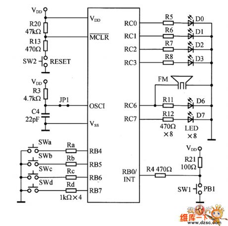
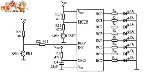
Clock circuit and reset circuit diagram
Published:2014/1/1 20:38:00 Author:lynne | Keyword: Clock circuit and reset circuit diagram,
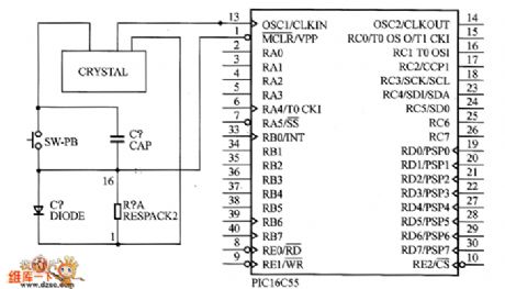
Clock circuit and reset circuit diagram shown in Figure:
(View)
View full Circuit Diagram | Comments | Reading(894)
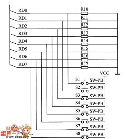
Determinant 4 × 4 keyboard circuit diagram
Published:2014/1/1 20:37:00 Author:lynne | Keyword: Determinant 4 × 4 keyboard circuit diagram,
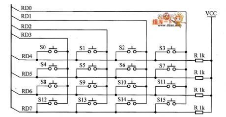
Determinant 4 × 4 keyboard circuit diagram shown in Fig.:
(View)
View full Circuit Diagram | Comments | Reading(965)
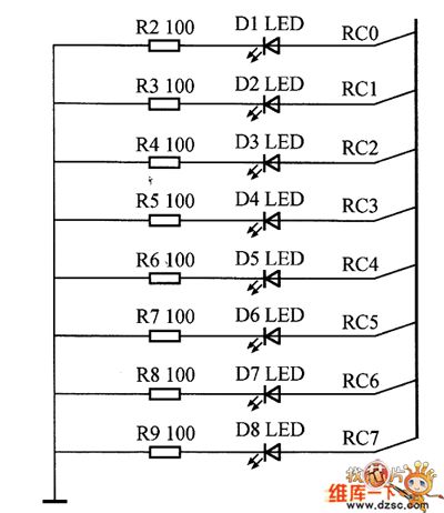
low four output of port C circuit diagram
Published:2014/1/1 20:35:00 Author:lynne | Keyword: low four output of port C circuit diagram,
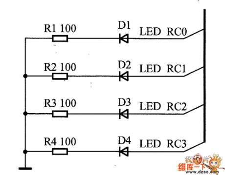
low four output of port C circuit diagram as shown in figure:
(View)
View full Circuit Diagram | Comments | Reading(804)
Applied voltage detection reset circuit schematics constructed by the IMP811
Published:2013/12/30 20:05:00 Author:lynne | Keyword: Applied voltage detection reset circuit schematics constructed by the IMP811, IMP811
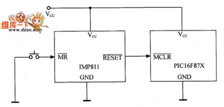
Applied voltage detection reset circuit schematics constructed by the IMP811 as shown in Figure:
(View)
View full Circuit Diagram | Comments | Reading(902)
RB port circuit diagram
Published:2013/12/30 20:07:00 Author:lynne | Keyword: RB port circuit diagram,
RB port circuit diagram shown in Figure:
(View)
View full Circuit Diagram | Comments | Reading(874)
Running water light circuit diagram
Published:2013/12/30 20:09:00 Author:lynne | Keyword: Running water light circuit diagram,
Running water light circuit diagram shown in Figure:
(View)
View full Circuit Diagram | Comments | Reading(1231)
The output display circuit diagram|
Published:2013/12/30 20:11:00 Author:lynne | Keyword: The output display circuit diagram,
The output display circuit diagram as shown:
(View)
View full Circuit Diagram | Comments | Reading(881)
Input circuit diagram
Published:2013/12/30 20:13:00 Author:lynne | Keyword: Input circuit diagram,
Input circuit diagram as shown:
(View)
View full Circuit Diagram | Comments | Reading(811)
The bus non-contact IC card read and write, circuit diagram
Published:2013/12/17 2:11:00 Author: | Keyword: The bus non-contact IC card read and write, circuit diagram,
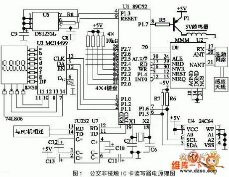
Bus non-contact IC card read and write device circuit diagram as shown below:
(View)
View full Circuit Diagram | Comments | Reading(1008)
Electronic exchange regulator magnetic amplifier circuit
Published:2013/12/12 20:15:00 Author:lynne | Keyword: Electronic exchange regulator magnetic amplifier circuit,

Electronic exchange regulator magnetic amplifier circuit shown in Figure:
(View)
View full Circuit Diagram | Comments | Reading(1281)
IC CA3130 Circuit
Published:2013/12/2 21:03:00 Author:lynne | Keyword: IC CA3130 Circuit
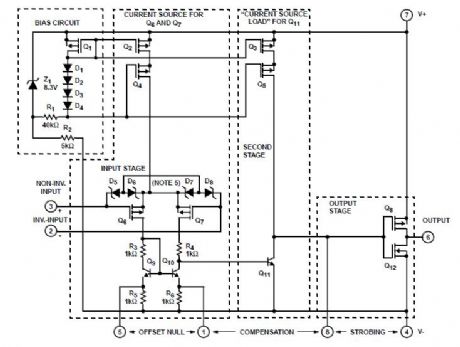
CA3130A and CA3130 are op amps that combine the advantage of both CMOS and bipolar transistors. Gate-protected P-Channel MOSFET (PMOS) transistors are used in the input circuit to provide very-high-input impedance, very-low-input current, and exceptional speed performance. The use of PMOS transistors in the input stage results in common-mode input-voltage capability down to 0.5V below the negative-supply terminal, an important attribute in single-supply applications.The CA3130 Series circuits operate at supply voltages ranging from 5V to 16V, (±2.5V to ±8V). They can be phase compensated with a single external capacitor, and have terminals for adjustment of offset voltage for applications requiring offset-null capability. Terminal provisions are also made to permit strobing of the output stage. The CA3130A offers superior input characteristics over those of the CA3130.
(View)
View full Circuit Diagram | Comments | Reading(1339)
TL071, TL072, TL074 Circuit
Published:2013/12/1 20:34:00 Author:lynne | Keyword: TL071, TL072, TL074 Circuit
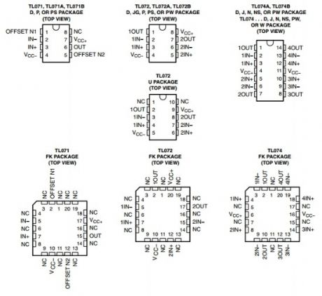
The JFET-input operational amplifiers in the TL07x series are similar to the TL08x series, with low input bias and offset currents and fast slew rate. The low harmonic distortion and low noise make the TL07x series ideally suited for high-fidelity and audio preamplifier applications. Each amplifier features JFET inputs (for high input impedance) coupled with bipolar output stages integrated on a single monolithic chip.TL071, TL072, TL074 Pinout
(View)
View full Circuit Diagram | Comments | Reading(1968)
Hi-Fi Stereo Preamp Circuit
Published:2013/11/28 20:56:00 Author:lynne | Keyword: Hi-Fi Stereo Preamp Circuit
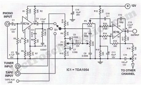
This Hi Fi stereo preamplifier circuit is built with TDA1054 IC from SGS. TDA1054 is a 16-pin DIL package and integrates 2 separate preamp circuits.It is a low noise preamp with little or no problem in the building process.The first half of the circuit (IC1a) it has an input sensitivity of 3 mV and has a frequency correction composed of C5, C3, R6 and R8. The bass signal coming from phono input is amplified while the high signal is attenuated.
The selection of the input signal sources is done with switch S1. P1 and P2 are parte of a double potentiometer. They control the high tones and bass. There is no risk of overdrive in circuit due to the passive nature of the sound control.
P3 controls the volume of the signal fed to se second part of the circuit (IC1b) which functions as an operational amplifier.
P4 controls the balance between the left and right channels but in the schematic is shown only the preamp for one channel.Both channel have a gain of 24 at the middle setting of P4. If P4 is set to one extreme end, the gain difference between the 2 channels is about 12 dB.
HiFi stereo preamplifier schematic
(View)
View full Circuit Diagram | Comments | Reading(1984)
LM317 Audio Amplifier Circuit
Published:2013/11/21 0:20:00 Author:lynne | Keyword: Audio Amplifier
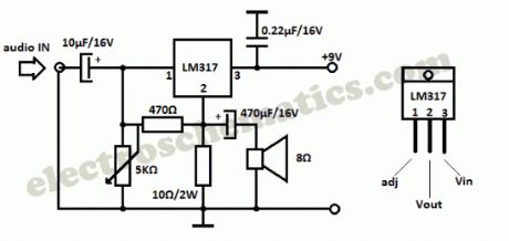
You probably know that LM317 IC is used as an adjustable voltage regulator, but did you know it can be used as an audio amplifier? This is a class A audio amplifier built with LM317 that delivers a maximum 1W audio power.
Use a good heatsink for the LM317 IC and adjust the 5K variable resistor so that you have 4.5V on 10Ω resistor (or LM317 pin 2, Vout).
LM317 amplifier schematic
(View)
View full Circuit Diagram | Comments | Reading(3962)
1W Audio Amplifier With Voltage Regulators
Published:2013/11/19 20:44:00 Author:lynne | Keyword: 1W Audio Amplifier
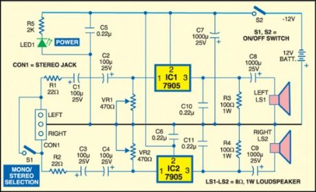
A simple stereo audio amplifier is built around two 7905 negative-voltage regulators (IC1 and IC2) and a few discrete components. The circuit will also work with other 79XX regulators if appropriate power supply is used. Regulator IC 7905 works as an amplifier for the voltages applied to common pin2 (Ground or GND). Also check the LM317 audio amplifier, another interesting circuit.
The minimal voltage drop over the standard 7905 is around 2V and it depends on the output current. Feedback resistors in the IC set the gain of the channel internally. The amplifier is a class-A audio amplifier. The minimal applicable value of R3 for the regulator 7905 is 8.2 to 10 ohms per 5W.
7905 1 Watt Audio Amplifier Schematic
If the required output current for LS1 is below 100 mA, the value of resistor R3 can be 33 to 51 ohms per watt. The circuit works with any load resistance (R3 in parallel with LS1 as the load) under the condition that the regulator is not overloaded with current and power dissipation. However, it is preferable to use a loudspeaker with a high resistance (8 ohms, 16 ohms or more). The amplifier works well with low-impedance headphones having a resistance of 24 to 32 ohms. The voltage difference between the ground pin of 7905 and the output pin is fixed internally.
S2 is the on/off switch. Switch S1 is for mono/stereo selection. When switch S1 is closed, the amplifier works as a two-way mono amplifier. If S1 is open, the amplifier works as a stereo amplifier. If no input signal is applied, the DC voltage on the output of the regulator 7905 should be around –5V, which depends to some extent on the value of VR1. The maximum output current of 7905 can be up to 1A and the maximum power dissipation is up to 15W. Mount the regulator IC 7905 on a heat-sink with thermal resistance below 15°C/W. (View)
View full Circuit Diagram | Comments | Reading(2961)
How to Move a Trip Point of Op-Amp Comparator Circuits
Published:2013/11/12 20:02:00 Author:lynne | Keyword: Op-Amp Comparator
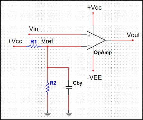
You all will befamiliar of basic comparator using a Op-Amp circuit. So today we will show you how to move a trip point of a Op-Amp comparator circuit. Maybe many of people already know this, but still this is the post forbeginners. So if you already know quit reading now only.
As shown in the above circuit, by application of a reference voltage to the inverting input rather than grounding it the trip can be moved. The reference voltage is given to the inverting input of a basic comparator using a potential divider consisting of resistors R1 and R2. The reference voltage Vref is derived using +Vcc and potential divider R1 and R2. Mathematically Vref is expressed as,
Vref = [+Vcc/(R1+R2)] R2
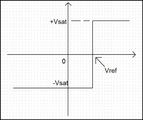
Now as long as the input voltage is less than Vref, the output is low i.e. -Vsat. When Vin becomes slightly greater than Vref, the Op-Amp output becomes high i.e. +Vsat. Thus the trip point is moved from Vin = 0 to Vin = Vref due to reference voltage applied to the inverting input terminal.
A bypass capacitor is used on the inverting input to reduce the amount of power supply ripple and noise appearing at the inverting input of Op-Amp. For effective bypassing of ripple and noise, the critical frequency of bypass circuit must be much lower than the ripple frequency of power supply.
The transfer characteristics of such a comparator is shown in above diagram which indicates positive trip point. Such a comparator is also called a limit detector as it detects the particular positive level of the input beyond which input goes high. The resistance R1 and R2 can be used to set the trip point anywhere between 0 and +Vcc.
The cut-off frequency of bypass circuit is,
fc = 1/[ 2π(R1||R2) Cby.
This must be much lower than the ripple frequency of the supply. (View)
View full Circuit Diagram | Comments | Reading(1660)
12V SCR Battery Charger Circuit
Published:2013/11/10 20:06:00 Author:lynne | Keyword: SCR Battery Charger Circuit
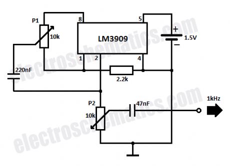
You can build a simple 1KHz square wave generator using a few components and the LM3909 that is useful for testing audio equipment. It is powered from a single 1.5V battery cell and the maximum amplitude of the output signal is 1.1V. With P1 you can adjust the symmetry of the square wave signal and with P2 the amplitude.Square wave generator schematic
(View)
View full Circuit Diagram | Comments | Reading(1266)
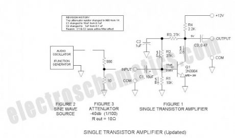
Single Transistor Amplifier Revisited – Part 3
Published:2013/10/31 22:14:00 Author:lynne | Keyword: Single Transistor, Amplifier
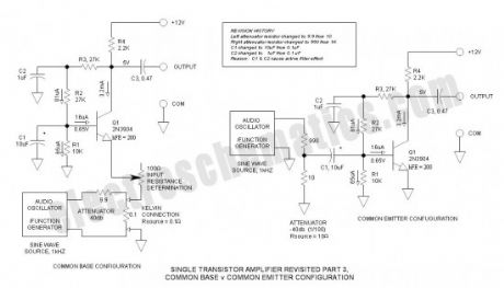
Single Transistor Amplifier Revisited Part 3, Common Base vs Common Emitter Configuration, Update
One nagging question that I have long had is this: How does the common base compare with the common emitter configuration in voltage gain performance? The classic microphone circuit interfaces a loudspeaker (used as microphone) directly to the emitter of a common base amplifier. My initial guess was that the difference would be negligible. However, when I wired and compared the two circuits, I learned a few new things.
Single Transistor Amplifier Schematic
Immediately, I learned that the common base configuration gain was 6db lower than the common emitter. This blew my mind. Then I started checking input resistance and was shocked at how low it measured (8.5Ω). I had previously guessed that it would be about 100Ω. Then I plotted the common base input resistance beside the common emitter input resistance — very useful information. The gain was 6db lower in the common base configuration because the source resistance almost exactly equaled the input resistance.
To obtain reliable input resistance data, I had to reduce the source resistance to 0.1Ω and connect via a Kelvin connection. Input resistance is surprisingly easy to determine experimentally by simply adding a pot between the low impedance voltage source and the amplifier input. Short the resistance and measure AC output voltage. Then increase resistance until the output voltage is exactly half. At this point, the pot resistance equals the input resistance and can be measured by a DMM.
Preface to the update
The initial data was in error due to a near resonant effect in the amplifier—this resonance caused unusually high voltage gain. After correcting the problem, I retook the data and updated the report.
I wish to acknowledge the contribution of Mr. Colin Mitchell who flagged an error regarding coupling capacitor (C1) size. Since this circuit was tested at 1 to 2kHZ, I figured that the capacitor value was not an issue. However, when C1 was increased to 10 uF, the gain unexpectedly decreased. This indicated an additional problem which turned out to be an active filter effect that also involved C2. When C1 and C2 were 0.1uF, the circuit resonated at the 2kHZ test frequency — almost all the elements of a phase shift oscillator were present. This is clear evidence of the veracity of Murphy’s Law — how could all these conditions occur at random?
As a result, Parts 1 and 2 had to be updated as well. (View)
View full Circuit Diagram | Comments | Reading(1376)
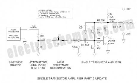
Single Transistor Amplifier Revisited – Part 2
Published:2013/10/20 20:23:00 Author:lynne | Keyword: Single Transistor , Amplifier
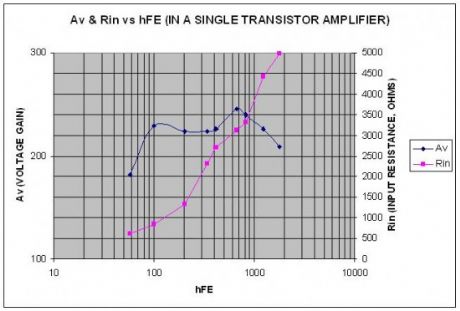
The goal of this series is to maximize the voltage gain of the single transistor amplifier. I had always thought that hFE had a profound effect upon voltage gain, so I set out to determine how much—the results surprised me. Then I went through another exercise to determine input resistance (Rin)—this is a grey area to most.
Graph of Voltage Gain & Input Resistance as a function of hFE
Transistor Selection
A number of transistors were added to those used in Part 1. This included a MPS6515 and a suspected “hot device” MPSA18 that turned out to be not as hot as I had predicted. Also, I added a 2N5088 and two very high hFE D3854 sample transistors that I had obtained from General Electric over 30years ago…no specs for this device can be found on the web, but I had had the foresight to write the hFE on the bag (hFE = 1500 to 3000).
Preface to the update
The initial data was in error due to a near resonant effect in the amplifier—this resonance caused unusually high voltage gain. After correcting the problem, I retook the data and updated the report.
Av is surprisingly stable
I would have thought with so wide a selection of transistors (nine in all), with a great range of manufacturers, packages, manufacturing dates, voltage ratings, current ratings, etc. that the curve would be lumpy with at least one or two anomalies that could not connect properly. However, such was not the case because it is apparent that voltage gain is largely independent of hFE. Note that the external circuit parameters likely have a significant effect, so any duplication of this exercise must be made under the same conditions.
Why the quest for high Av? Everyone wants “hot” amplifiers—gutless amplifiers are depressing. Perhaps you do not need all this voltage gain—in that case, it can be used to reduce distortion and noise via negative feedback—I am not suggesting that this open loop amplifier has low distortion—we will discuss that in future parts. Also, the conclusion of this series will introduce an amplifier with incredible gain performance.
Effective Av with a 2.2K resistor @ 3.2mA is approx 225—keep this number in mind.
Schematic of test setup
(View)
View full Circuit Diagram | Comments | Reading(1488)
Single Transistor Amplifier Revisited – Part 1
Published:2013/10/11 20:51:00 Author:lynne | Keyword: Single Transistor Amplifier Revisited – Part 1
Circuit and Biasing Technique
There is so much to learn about the single-transistor amplifier, that this brief tutorial hardly scratches the surface. This discussion considers only the common-emitter configuration as applied to low level audio.
History
In the early days of solid state amplifiers, thermal stability was the big issue. The first devices available were leaky germanium PNP transistors. The collector to base leakage was often so excessive that it could cause thermal run-away because the leakage increased exponentially with temperature. The classic way of keeping this under control was the base divider-emitter swamping resistor topology. Early text books (including the one I used in 1963) had a detailed section on this and included a mathematical calculation for “stability factor.”
Unfortunately, now (some 50 years later), we are still suffering from vestiges of this approach as we continue to see the same circuits popping up even though germanium transistors have been obsolete and unavailable for well over 30years, and the silicon bipolar NPN has been long the transistor of choice. Since leakage in silicon devices is so low that it can hardly be measured, we can make a fresh start.
Self-Biased Circuit Schematic
A stable quiescent operating point (“Q” point) can be established simply by sourcing the base divider from the collector voltage. This dispenses with the emitter swamping resistor. While not perfect, it provides predictable results and simplicity. It is good for low power amplifier transistors that dissipate less than about 100mW. R1, 2 & 3 form the base divider. The juncture of R2 & 3 is bypassed to common via C2 to eliminate negative feedback from the collector—this negative feedback tends to reduce voltage gain. We will be covering negative feedback in the future. C1 is the input coupling capacitor and C3 is the output coupling capacitor—both pass the AC signal while blocking the DC component. To accommodate a wide range of hFE’s, the base divider current is in the range of 5 to 10 * base current.
Operating point calculations (ohms law)
Set collector voltage: My rule-of-thumb is to set it at about 40% of Vcc. In this case it is 5V.
Calculate collector current: Ic = (Vcc – Vc) /R4 = (12V – 5V) /2.2K = 3.2mA.
Calculate base current: Ib = Ic / hFE = 3.2mA /200 = 16uA (using the common 2N3904)
Establish base divider current: Id = Ib * 5 = 16uA * 5 = 80uA (a factor of 5 is good)
Calculate Ir1: Ir1 = Id – Ib = 80uA – 16uA = 64uA
Calculate R1: R1 = Vbe / Ir1 = 0.65V /64uA = 10K
Calculate R2 + R3: R23 = (Vc – Vbe) /Id = (5 – 0.65V) /80uA = 54K
Calculate R2,3: R2 = R3 = 54K / 2 = 27K (may be unequal, but total must be 54K) (View)
View full Circuit Diagram | Comments | Reading(1567)
| Pages:4/250 1234567891011121314151617181920Under 20 |
Circuit Categories
power supply circuit
Amplifier Circuit
Basic Circuit
LED and Light Circuit
Sensor Circuit
Signal Processing
Electrical Equipment Circuit
Control Circuit
Remote Control Circuit
A/D-D/A Converter Circuit
Audio Circuit
Measuring and Test Circuit
Communication Circuit
Computer-Related Circuit
555 Circuit
Automotive Circuit
Repairing Circuit