
Amplifier Circuit
Index 95
50_MC_40_w_POWER_AMPLIFIER
Published:2009/7/10 1:33:00 Author:May
Paralleled silicon transistors operanng as class C are biosed on by incoming r-f signal,hence stop conducting when there is no signal,-R.C.Heihall, Getting Transistors into Single-Side.band Amplifiers, Electonics,37:17,p 72-75. (View)
View full Circuit Diagram | Comments | Reading(756)
30_MC_LINEAR_SINGLE_SIDEBAND_AMPLIFIER
Published:2009/7/10 1:31:00 Author:May

Single silicon transistor with impedance matching network and pi output network delivers 20 w of r-f peak envelope power, with all odd-order distortion products at least 30 db down.-R. C. Heihall, Getting Transistors Into Single,Sideband Amplilers, Elecrronics, 37:17, p 72-75. (View)
View full Circuit Diagram | Comments | Reading(759)
COMPOUND_OP_AMP
Published:2009/7/10 1:28:00 Author:May
By using an emitter-follower or a Darlington pair, a voltage-follower op amp configuration can source higher currents than the op amp otherwise could. (View)
View full Circuit Diagram | Comments | Reading(2491)
3_INPUT_AND_GATE_COMPARATOR
Published:2009/7/10 1:18:00 Author:May
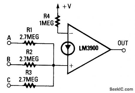
This circuit has high output onty when all three inputs are high. The noninverting-input current, when all three inputs are high, must exceed that of the inverting input, as determined by R4. The circuit can be converted to a NAND gate by transposing the two inputs of the op amp. (View)
View full Circuit Diagram | Comments | Reading(975)
MAKE_LM324_OP_AMP_SWING_RAIL_TO_RAIL
Published:2009/7/10 1:09:00 Author:May
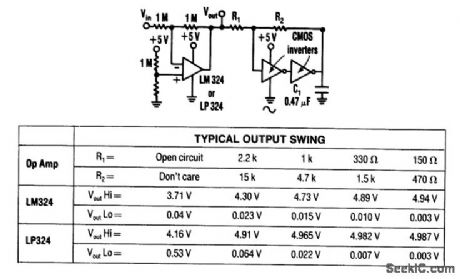
By using two CMOS inverters, the output for an LM324 op amp can be increased from 3.5 Vpp to 4.9 Vpp. This circuit is only recommended for light loads (<30 mA) and for relatively slow op amps. Any CM0S inverter (74C00, 74C02, 74C14, CD4001, CD4011, etc.) can be used. (View)
View full Circuit Diagram | Comments | Reading(1592)
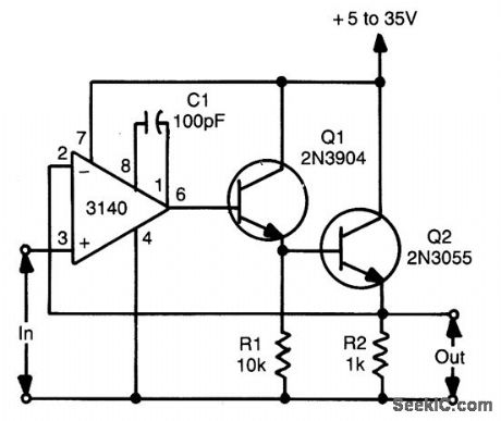
BIDIRECTIONAL_COMPOUND_OP_AMP
Published:2009/7/10 0:51:00 Author:May
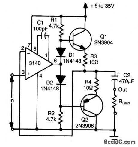
Using two transistors (Q1 and Q2), a bidirec-tional op amp can source or sink up to 50 mA. D1 and D2 provide bias for Q1 to eliminate dead-zone effects. (View)
View full Circuit Diagram | Comments | Reading(683)
GAIN_CONTROLLED_OP_AMP
Published:2009/7/10 0:46:00 Author:May
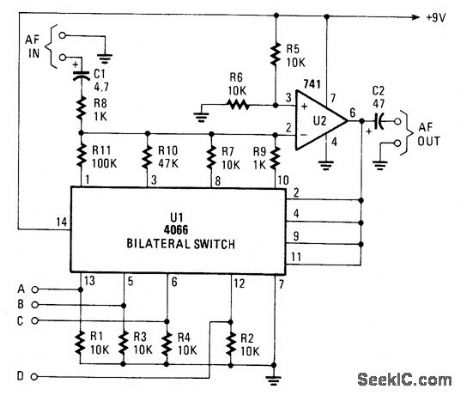
The gain controller uses a 4066 quad bilateral switch to electronically select a feedback resistor for the 741 op amp. One or more switches can be turned on at the same time to produce a stepped, variable-gain range from less than 1 to 100. (View)
View full Circuit Diagram | Comments | Reading(3562)
INCREASED_FEEDBACK_STABILIZED_AMPLIFIER
Published:2009/7/10 0:41:00 Author:May
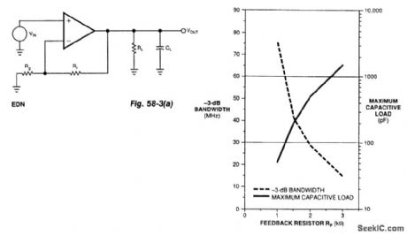
The usual method for using a current-feedback amplifier to drive a capacitive load isolates the load with a resistor in series with the amplifier's output.
A better solution involves only the amplifier's feedback resistors (Fig. 58-3(a)). Because the feedback resistors determine the amplifier's compensation, you can select the optimal value for these feedback resistors for almost any capacitive load.
Feedback resistance RF sets the amplifier's bandwidth. Increasing RF reduces the amplifier's band-width, which significantly improves the amplifier's ability to drive capacitive loads. Feedback resistor RG sets the amplifier's gain.
You cannot get the data necessary to calculate alternate values for RF from most data sheets. How-ever, a few minutes at the bench with a network analyzer will generate the data to make a graph of the value of the feedback resistor vs. the amount of capacitive load the amplifier can drive (Fig. 58-3(b)).
Start with the recommended data-sheet value for feedback resistor RF and measure the amplifier's frequency response without any capacitive load. Note the bandwidth, then add capacitive loading until the response peaks by about 5 dB. Record this value of capacitance; it is the maximum amount for that feed-back resistor. Then, increase the value of the feedback resistor and repeat the procedure until you develop a graph like the one in Fig. 58-3(b). (View)
View full Circuit Diagram | Comments | Reading(707)
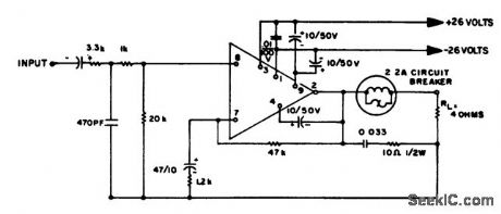
13_watt_AF_power_amplifier_designed_for_an_8_ohm_or_4_ohm_load
Published:2009/7/20 1:49:00 Author:Jessie
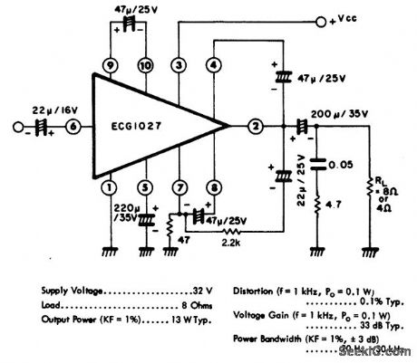
13-watt AF power amplifier designed for an 8-ohm or 4-ohm load. The circuit needs only one power supply rated at 32 volts, 50 mA (courtesy GTE Sylvania Incorporated). (View)
View full Circuit Diagram | Comments | Reading(706)
JFET_WIDEBAND_AMPLIFIER
Published:2009/7/10 0:37:00 Author:May
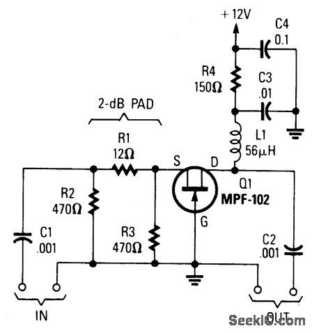
Using an MPF102 JFET, this circuit has a 50-Ω input impedance。Load impedance should be about 470Ω. A 3∶1 matching transformer can be used to get the impedance back to 50 Ω,This circuit will showabout 6- to 8-dB gam at VHF frequencies. (View)
View full Circuit Diagram | Comments | Reading(2388)
2_watt_AF_phono_amplifier_using_an_ECG740A_14_pin_DIP
Published:2009/7/20 1:48:00 Author:Jessie
2-watt AF phono amplifier using an ECG740A 14-pin DIP. Supply voltage is typically 18 volts. Voltage gain is 34 dB. Minimum audio power output is 2 watt, with 2.5 watts typical. When driving a 16-ohm load the supply voltage at pin 14 should be 24 volts (courtesy GTE Sylvania Incorporated). (View)
View full Circuit Diagram | Comments | Reading(769)
MOSFET_WIDEBAND_AMPLIFIER
Published:2009/7/10 0:35:00 Author:May
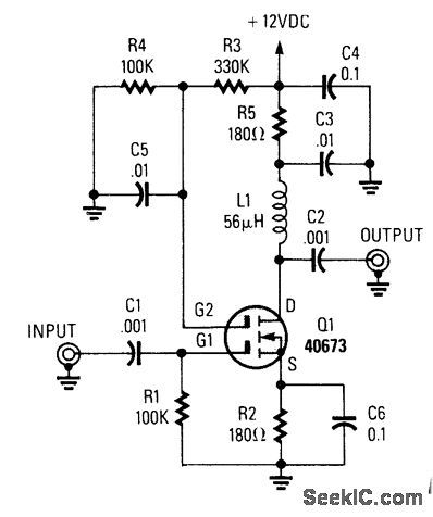
For high-impedance (7500 Ω) applications, this amplifter will provide a voltage gain of approximately -gm/ZL where ZL is the load impedance in ohms and gm is ≈ 12 x 10-3 for the 40673 FET. The G2 voltage can be used to control the gain. (View)
View full Circuit Diagram | Comments | Reading(1450)
HF_WIDEBAND_AMPLIFIER
Published:2009/7/10 0:34:00 Author:May
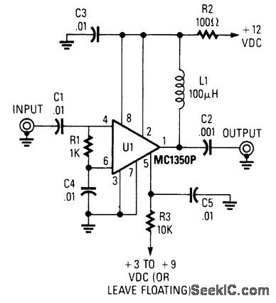
About 20-dB gain can be obtained using this IC. The gain can be controlled by varying the voltage applied to R3. (View)
View full Circuit Diagram | Comments | Reading(833)
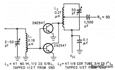
500_MHz_AMPLIFIER
Published:2009/7/10 0:33:00 Author:May
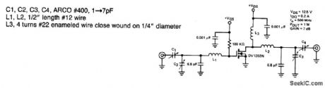
This amplifier provides 1-W output at 500 MHz with a DV1202W FET. About 6- to 8-dB power gain can be expected. (View)
View full Circuit Diagram | Comments | Reading(786)
TWO_CA3100_WIDEBAND_OPERATIONAL_AMPLIFIERS
Published:2009/7/10 0:32:00 Author:May
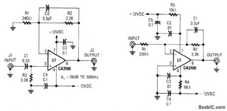
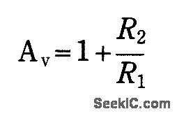
These circuits use the RCA CA3100 wideband amplifier IC. The gain is:These circuits are useful for video applications to 10 MHz. The 3.3-pF capacitors are compensation capacitors. Capacitors on pins 7 and 4 are bypass capacitors to prevent self-oscillations. Figure 76-18(a) is noninverting and Fig. 76-18(b) is an inverting configuration. (View)
View full Circuit Diagram | Comments | Reading(705)
Stereo_phono_AF_preamplifier_for_magnetic_pickups_using_the_ECG727
Published:2009/7/20 1:45:00 Author:Jessie
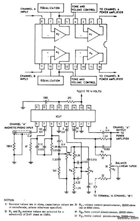
Stereo phono AF preamplifier for magnetic pickups using the ECG727. The schematic shows only one channel. Duplicate components must be used for channel B. Refer to the block diagram for pin identification. Voltage gain at t kHz is 47 dB. The ECG727 has four internal AC amplifiers (courtesy GTE Sylvania Incorporated). (View)
View full Circuit Diagram | Comments | Reading(689)
OP_AMP_REGULATOR
Published:2009/7/10 0:03:00 Author:May


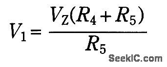


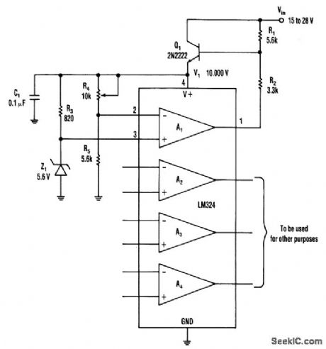
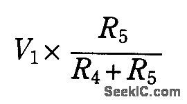


This op amp offers a straightforward method of developing a single-polarity stable voltage source (see the ftgure). Transistor Q1 gets a base drive through resistor R1, and conducts to develop a voltage(V1) across the IC's supply pins. Amp A1, R2, and Q1 form a positive-feedback closed loop, along with R3 and the zener diode. A1, R2, and Q1 also form a negative-feedback closed loop with R4 and R5.The effect of positive feedback is predominant as the noninverting input receives V1while the inverting input receives only: This happens until the zener comes into play. When the voltage at the inverting input exceeds the voltage at the noninverting input, A1's output takes away Q1's base current through R2, which reduces V1.Hence, an equilibrium condition is reached. Now:This circuit can source more than 30 mA. (View)
View full Circuit Diagram | Comments | Reading(1014)
MULTIPLYING_PRECISE_COMMUTATING_AMP
Published:2009/7/9 23:55:00 Author:May
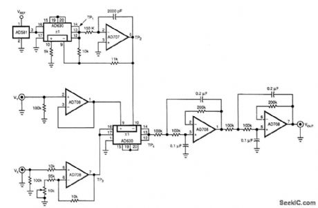
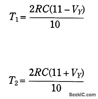
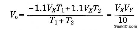
By using a pulse-width-height modulation technique, this circuit implements a 0.015%-accurate multi-plier. The circuit's output equals VXVY/10. An AD581 voltage reference, an AD630 commutating amplifier, and an integrator comprising an AD707 op amp, 2000-pF capacitor, and 150-kΩ resistor first generate a precision triangle wave. For a given state of the AD630's output (+VREF at TP1, for example) the integra-tor ramps until its output reaches -11V. Then, TP) changes state and the integrator begins ramping toward +11V. The triangle wave's period is 4.4RC or 1.32ms, where R and C are the values of the integrator components.
The circuit uses a second AD630, driven by the variable VX to compare the triangle waveform at TP2 to the signal at VY The duty cycle, T1+T2, at the output of this second commutating amplifier is:
During T1, the voltage at TP4 equals -1.1VX. During the remaining period, T2, the pulse height will equal+1.1VX. VOUT is the average, obtained by low-pass filtering, of this T1 and T2 combined waveform and equals:
You can use a higher bandwidth filter and a higher carrier frequency to build a faster multiplier. (View)
View full Circuit Diagram | Comments | Reading(988)
Low_noise_equalizing_amplifier_using_an_ECG1019_thin_film_hybrid_module
Published:2009/7/20 2:46:00 Author:Jessie

Low-noise equalizing amplifier using an ECG1019 thin-film hybrid module (courtesy GTE Sylvania Incorporated). (View)
View full Circuit Diagram | Comments | Reading(785)
15_watt_AF_power_amplifier_using_an_ECG1028_module
Published:2009/7/20 2:45:00 Author:Jessie
15-watt AF power amplifier using an ECG1028 module. An ECG1090 module can be substituted for the ECG1028 by omitting the 20K resistor at pin 8 and the 47K resistor between pins 7 and 2 (courtesy GTE Sylvania Incorporated). (View)
View full Circuit Diagram | Comments | Reading(798)
| Pages:95/250 At 2081828384858687888990919293949596979899100Under 20 |
Circuit Categories
power supply circuit
Amplifier Circuit
Basic Circuit
LED and Light Circuit
Sensor Circuit
Signal Processing
Electrical Equipment Circuit
Control Circuit
Remote Control Circuit
A/D-D/A Converter Circuit
Audio Circuit
Measuring and Test Circuit
Communication Circuit
Computer-Related Circuit
555 Circuit
Automotive Circuit
Repairing Circuit