
Amplifier Circuit
Index 84
CONTROL_AMPLIFIER
Published:2009/7/11 4:50:00 Author:May
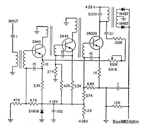
Converts output of 20-kc chopper to d-c error signal.Amplifier output is rectified by diodes rather than demodulated,since polarity of error is of no concern.-J.W.Higginbotham and H.H.Douglass.Voltage Comparator with High-Speed Switches,Electronics.32:5,p56-58 (View)
View full Circuit Diagram | Comments | Reading(637)
DIFFERENTIAL_VOLTAGE_COMPARATOR
Published:2009/7/11 4:34:00 Author:May
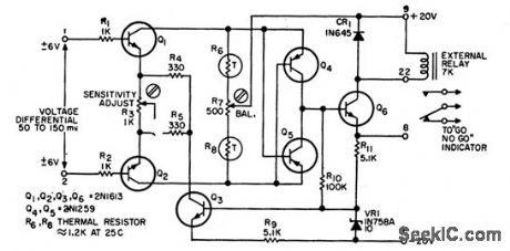
If the two input signals are within preset differential voltage relay is not actuated and GO indicator comes on.When the two signal differ too much,relay is actuated and NO-GO indication is provided.Used in commparing telemetered data received from satellite vehicle.-P.A.Walter,Differential Voltage Comparator.EEE.10:8,p24-25 (View)
View full Circuit Diagram | Comments | Reading(765)
TUNNEL_DIODE_VOLITAGE_COMPARATOR
Published:2009/7/11 4:27:00 Author:May
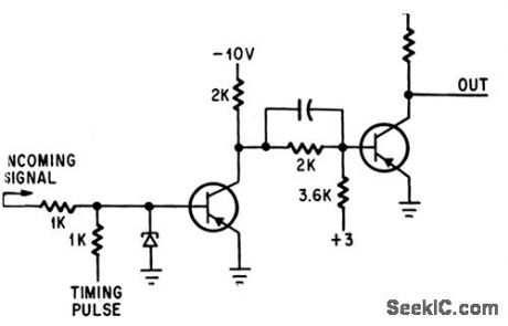
When incoming signal exceeds predetermined leverl,pulse with predetermined amplitude appears at output.-T.Kolima and M.Watanabe,When You're Second,You Try Harder,Electronics,38:25,p81-89 (View)
View full Circuit Diagram | Comments | Reading(730)
AGC_amplifier
Published:2009/7/17 3:00:00 Author:Jessie
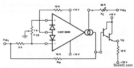
This circuit uses one section of an XR-13600 (Fig. 11-1B) as an AGC amplifier. When VO reaches a high enough amplitude to turn the Darlington transistors and linearizing diodes, the increase in ID reduces amplifier gain so as to hold VO at that level. The control point is set by RC and the output offset is adjusted by the 1 -kΩ potentiometer. (View)
View full Circuit Diagram | Comments | Reading(0)
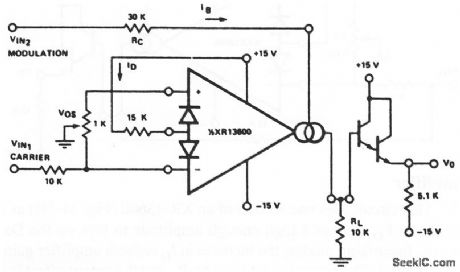
Four_quadrant_multiplier
Published:2009/7/17 2:58:00 Author:Jessie
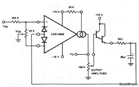
This circuit uses one section of an XR-13600 (Fig. 11-1B) as a four-quadrant multiplier. Notice that the output is taken from the amplifier, and that the buffer output is returned to the amplifier input. The 100-kΩ potentiometer sets the output amplitude and the 25-kΩ potentiometer is used to adjust offset. (View)
View full Circuit Diagram | Comments | Reading(0)
Logarithmic_amplifier_using_an_MC1556_op_amp_1
Published:2009/7/17 2:56:00 Author:Jessie

Logarithmic amplifier using an MC1556 op amp (courtesy Motorola Semiconductor Products Inc.). (View)
View full Circuit Diagram | Comments | Reading(848)
Logarithmic_amplifier_using_an_MC1556_op_amp
Published:2009/7/17 2:55:00 Author:Jessie
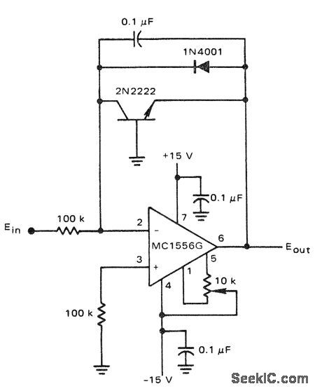
Logarithmic amplifier using anMC1556 op amp. The 10K pot is an offset adjustment (courtesy Motorola Semiconductor Products Inc.). (View)
View full Circuit Diagram | Comments | Reading(835)
Voltage_controlled_amplifier
Published:2009/7/17 2:50:00 Author:Jessie

This circuit uses one section of an XR-13600 dual OTA as a voltage controlled amplifier. Figure 11-1B shows that both sections of the XR-13600 have predistortion diodes and noncommitted Darlington buffer outputs. In the circuit of Fig. 11-1A, the bias current IB(pins 1 and 16) controls gain of the output. The 1-kΩ potentiometer at the amplifier input is adjusted to minimize the effects (offset) of the gain-control signal at the output. ExAP corporaton Databook, 1990, p 524S 5-252 (View)
View full Circuit Diagram | Comments | Reading(0)
Stereo_volume_control
Published:2009/7/17 2:48:00 Author:Jessie
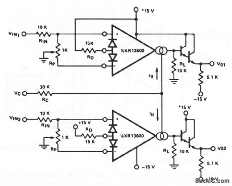
This circuit uses both sections of an XR-13600 (Fig. 11-1B) as a stereo volume control with typical channel-to-channel gain tracking of 0.3 dB. The RP potentiometers are provided to minimize the output offset voltage and they can be replaced with two 510-Ω resistors in ac-coupled applications. With the values shown, amplifier gain is: VO/VIN = 940× IB (mA). EXAR corporation Databook 1990 p 5-253 (View)
View full Circuit Diagram | Comments | Reading(1153)
IF_AMPLIFIERIER
Published:2009/7/17 2:47:00 Author:Jessie
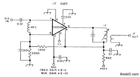
Using a CA3028A,this circuit is useful up to about 15 or 20 MHz. (View)
View full Circuit Diagram | Comments | Reading(1280)
Logarithmic_amplifier_using_an_MC1S39G_op_amp_
Published:2009/7/17 2:52:00 Author:Jessie
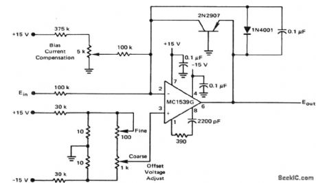
Logarithmic amplifier using an MC1S39G op amp (courtesy Motorola Semiconductor Products Inc.). (View)
View full Circuit Diagram | Comments | Reading(680)
Amplitude_modulator
Published:2009/7/17 2:52:00 Author:Jessie
This circuit uses one section of an XR-13600(Fig.11-1B)and an amplitude modulator (or two-quadrant multiplier), where IO=(-2IS/ID) ×(IB) EXAR Corporation Databook, 1990 p 5-253 (View)
View full Circuit Diagram | Comments | Reading(0)
AGC_SYSTEM_FOR_CA3028_IF_AMPLIFIER
Published:2009/7/17 2:45:00 Author:Jessie
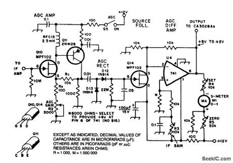
An MPF102 amplifier feeds IF signals to a 2N4126. A potentiometer in the MPF102 Source acts as agatn control.This voltage is rectified by an 1N914 doubling detector, and drives a 741 op amp vla a source follower(Q14).S-meter and IF-gain controls are provided. (View)
View full Circuit Diagram | Comments | Reading(2804)
STRAIN_GAGE_AMPIJFIER
Published:2009/7/17 2:45:00 Author:Jessie
Positive and negative feedback to bridge-type transformer coupled input circuit provides high-impedance looting differential input in d-c to 25-kc amplifier. Bridge balances out commonmode signals that arise in data acquisition systems, where pre-amplifier ground may be hundreds of feet from transducer ground. Floating output delivers low voltage at high current for recorder or analog-to-digital converter. Linearity is within 15 microvolts from d-c to 25 kc. Chopper stabilization keeps input d-c drift below 0.5 microvolt during 40-hour run.-R. S. Burwen, Amplifiers for Strain Gages and Thermocouples, Electron, ics, 32:30, p 43-45. (View)
View full Circuit Diagram | Comments | Reading(989)
High_impedance_bridge_amplifier_using_three_MC1556_op_amps
Published:2009/7/17 2:41:00 Author:Jessie
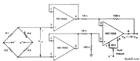
High-impedance bridge amplifier using three MC1556 op amps (courtesy Motorola Semiconductor Products Inc.). (View)
View full Circuit Diagram | Comments | Reading(712)
COMPARATOR_FOR_SOLID_SlAlE_DIGITAL_VOLTMETER
Published:2009/7/11 3:31:00 Author:May
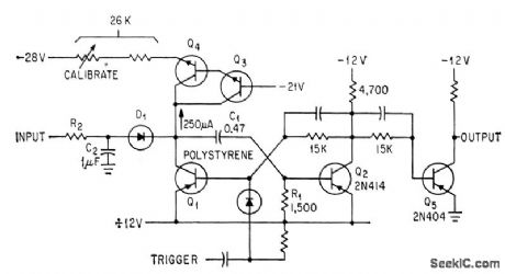
Circuit determines when output of ramp genercttor crosses 0V and crosses unknown voltage. Transistor Q5 isolates mono Q1-Q2 from output iogic. Iransistors Q3 amd Q4 provide constant current for charging C1 linearly to produce high-accurctcy ramp.-R.C. Weinberg, Modified Ramp Generator Develops High D-C input impedance, Electronics, 37:8, p33-35. (View)
View full Circuit Diagram | Comments | Reading(825)
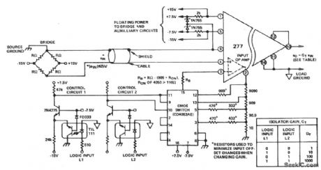
Programmable_gain_bridge_transducer_amplifier_
Published:2009/7/17 2:37:00 Author:Jessie
Programmable gain bridge transducer amplifier (courtesy Analog Devices, Inc.). (View)
View full Circuit Diagram | Comments | Reading(756)
Bridge_amplifier
Published:2009/7/17 2:36:00 Author:Jessie
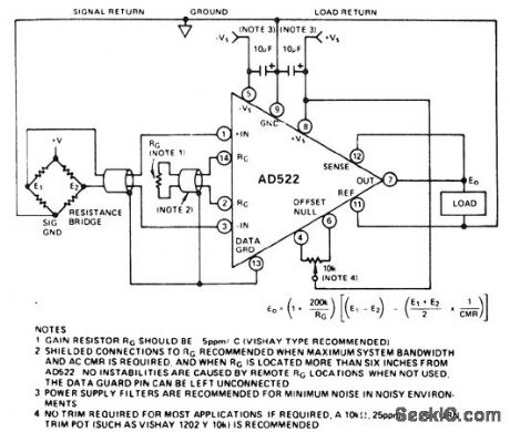
Bridge amplifier. Typical supply voltage is ±15 volts (courtesy Analog Devices, Inc.). (View)
View full Circuit Diagram | Comments | Reading(0)
VIDEO_LOOP_THRU_AMPLIFIER
Published:2009/7/11 3:02:00 Author:May
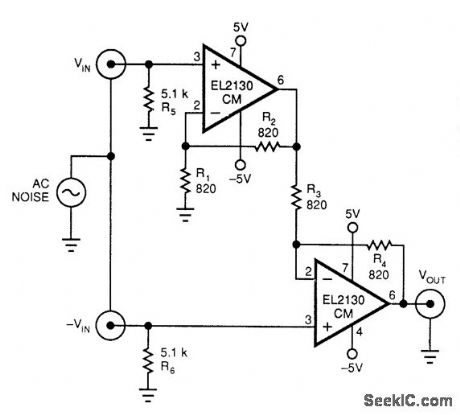
This video bandwidth amplifier rejects commonmode noise, such as 60- and 120-Hz hum. Bandwidth is typically 60 MHz for a differential gain of 2.The common-mode rejection is typically 45 dB.The design equations are:
ADIFF ≥ 1R2 = R4 (select both for optimum bandwidth)R1=R2 (ADlFF-1)R3=R4 (ADIEF-1) (View)
View full Circuit Diagram | Comments | Reading(728)
VIDEO_OP_AMP_CIRCUITS
Published:2009/7/11 2:54:00 Author:May
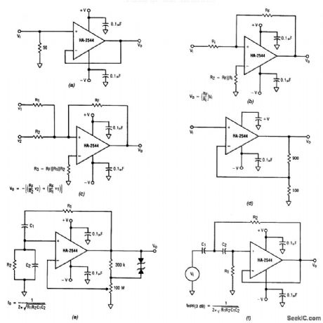
These 6 circuits use the Harris HA2544 op amp. Component values are obtained by using the equations in the figure.The HA-2544 can be used in any number of standard op amp configurations, including a voltage follower (a), an inverting amplifier (b), an inverting summer (g), a buffer amplifier with a gain of 10 (d), a Wien-bridge oscillator with zener diode adaptive feedback (e), and a second-order, high-pass active filter (f). (View)
View full Circuit Diagram | Comments | Reading(2528)
| Pages:84/250 At 2081828384858687888990919293949596979899100Under 20 |
Circuit Categories
power supply circuit
Amplifier Circuit
Basic Circuit
LED and Light Circuit
Sensor Circuit
Signal Processing
Electrical Equipment Circuit
Control Circuit
Remote Control Circuit
A/D-D/A Converter Circuit
Audio Circuit
Measuring and Test Circuit
Communication Circuit
Computer-Related Circuit
555 Circuit
Automotive Circuit
Repairing Circuit