
Amplifier Circuit
Index 97
5_W_150_MHz_AMPLIFIER
Published:2009/7/9 23:00:00 Author:May
This circuit utilizes the MRF123 TMOS power FET The MRF134 is a very high gain FET that is potentially unstable at both VHF and UHF frequencies. Note that a 68-Ω input loading resistor has been utilized to enhance stability. This amplifter has a gain of 14 dB and a drain efficiency of 55%. (View)
View full Circuit Diagram | Comments | Reading(821)
1_MHz_METER_DRIVER_AMPLIFIER
Published:2009/7/9 22:59:00 Author:May
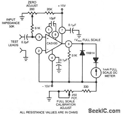
This circuit uses the CA3100 BiMOS op amp to drive a 1-mA meter movement to full scale with 1-V rms input. (View)
View full Circuit Diagram | Comments | Reading(714)
RF_WIDEBAND_ADJUSTABLE_AGC_AMPLIFIER
Published:2009/7/9 22:58:00 Author:May
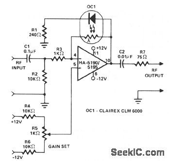
This circuit functions as a wideband adjustable AGC amplifier.With an effective bandwidth of approximately 10 MHz,it is capable of handling rfinput signal frequencies from 3.2 to 10 MHz at levels ranging from 40 mV up to 3 V pk-pk.AGC action is achieved by using optocoupler/isolater OC1 as part of the gain control-feedback loop.In operation, the positive peaks of the amplifed output signal drive the OC1 LED into a conducting state. Since the resistance of the OC1 photosensitive element is inversely proportional to light intensity, the higher the signal level, the lower the feedback resistance to the op amp inverting input. The greater negative feedback lowers stage gain. Any changes in gain occur smoothly because the inherent memory characteristic of the photoresistor acts to integrate the peak signal inputs. In practice, the stage gain is adjusted automatically to where the output signal positive peaks are approximately one diode drop above ground.Gain set control R5 applies a fixed dc bias to the op amp noninverting input, thus establishing the steady state-zero input signal current through the OC1 LED and determining the signal level at which AGC action begins.The effective AGO range depends on a number of factors, including individual device characteristics, the nature of the rf drive signal, the initial setting for R5, et al. Theoretically, the AGC range can be as high as 4000:1 for a perfect op amp because the OC1 photoresistor can vary in value from 1 MΩ with the LED dark to 250 Ω with the LED fully on. (View)
View full Circuit Diagram | Comments | Reading(2559)
450_MHz_COMMON_GATE_AMPLIFIER
Published:2009/7/9 22:52:00 Author:May
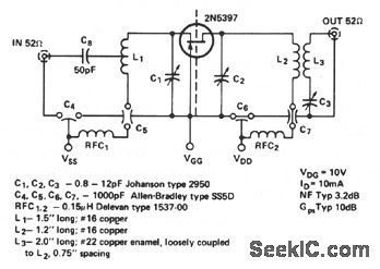
This is a low nolse,3-dB typical NF,amplifier with about 10-dB gain at 450-470 MHz for VHF two-way applications. (View)
View full Circuit Diagram | Comments | Reading(679)
2_30_MHz_AMPLIFIER
Published:2009/7/9 22:51:00 Author:May
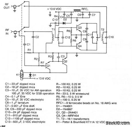
This amplifier provides 140-W PEP nominal output power when supplied with input levels as low as 3 W. Both input and output transformers have a 4:1 turn ratio and a 16:1 impedance ratio to achieve low input VSWR across the band with high-saturation capability. (View)
View full Circuit Diagram | Comments | Reading(805)
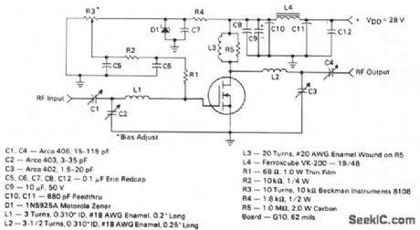
10_dB_GAIN_AMPLIFIER
Published:2009/7/9 22:50:00 Author:May
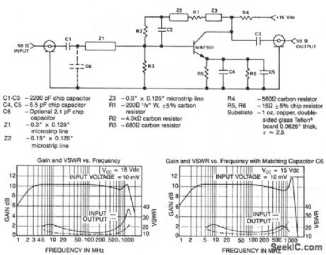
This circuit design is a class A amplifier employing both ac and dc feedback. Bias is stabilized at 15 mA of the collector current using dc feedback from the collector. The ac feedback, from collector to base, and in each of the partially bypassed emitter circuits, compensates for the increase in device gain with decreasing frequency, yielding a flat response over a maximum bandwidth. The amplifter shows a nominal 10-dB power gain from 3 MHz to 1.4 GHz. With only a minimum matching network used at the amplifier input, the input VSWR remains less than 2.5:1 to approximately 1 GHz, while the output VSWR stays under 2:1. Note that a slight degradation in gain flatness and output VSWR occurs with the addition of C6. A more elaborate network design would probably optimize impedance matching, while maintaining gain flatness. (View)
View full Circuit Diagram | Comments | Reading(1356)
1296_MHz_SOLID_STATE_POWER_AMPLIFIER
Published:2009/7/9 22:48:00 Author:May

The design incorporates 30-Ω,1/4λmicrostrip lines on the input and output.C3,C4,C7,and C8,along with L1, from a pi network that matches the low-input impedance ofthe device to 50 Ω.C5,C6,C9,C10,and 30-Ω transmission line L2 form an outputpl network that maxlmlzes power transfer to 50 Ω.C10 is not always necessary, depending on variations among devices and circuitboard material.Bias is provided by R1,R2,and D1.R1 can be optimized, if desired,to adjust the collector idling current. (View)
View full Circuit Diagram | Comments | Reading(1611)
UNIVERSAL_COMPANDER
Published:2009/7/9 22:41:00 Author:May
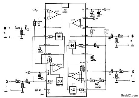
Signetics' type NE575 compander IC is intended primarily for use with battery power supplies of 3 to 7 V (max. 8 V). It draws a current of 3.5 mA at 3 V and 5 mA at 7 V. The compander process (compression at the input, expansion at the output) significantly improves the signal-to-noise ratio in a communications link.
The IC contains two almost identical circuits, of which one (pins 1 to 9) is arranged as an expander. The other (pins 11 to 19) can be used as expander, compressor or automatic load control (ALC), depend-ing on the externally connected circuit. For the compressor function, the inverting output of the internal summing amplifier is brought out to pin 12. This is not the case in the expander section, where a reference voltage is available at pin 8. This pin is interlinked to pins 1 and 19 to enable the setting of the dc operating point of the op amps.
The op amp in the expander section, pins 1 through 3, serves as output buffer in the compressor section, pins 17 through 19 as the input buffer. The IC has a relatively high output sensitivity and is evi-dently intended for processing small signals (microphone output level). A signal of 100 mV, for instance, is amplified by 1 only. The present circuit caters to larger input signals (line level); its maximum input level is 1.5 Vrms.
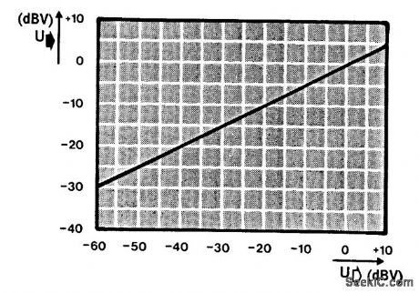
With a 1-V input into R13, a potential of about 500 mV exists between compressor output R7 and expander input R5. The compression characteristic is shown in Fig. 19-2(b). The signal range is reduced by about one half at the output, which is doubled in the expander. Thus, the range after compression and expansion is the same again, but that is not necessarily the case with the input and output level. The com-pander can be arranged to provide a constant attenuation or amplification. With the circuit values as shown in the diagram, the input and output levels are the same. The prototype had an overall gain of 0.5 dB when the expander input was connected directly to the compressor output.
To allow acceptance of high input levels, R13, R14, and the compressor input resistance form a 10:1 attenuator. At the expander input, R5 and the expander input impedance of about 3 k0 form a potential divider. If the compander is to be used with smaller signals, the attenuation can be reduced as appropriate. If the input level lies below 100 mV, R5, R13 and R14 can be omitted.
The compander covers the frequency range of 20 Hz to 20 kHz, the overall distortion is less than 1%, and the signal-to-noise ratio is about 80 dB. (View)
View full Circuit Diagram | Comments | Reading(1955)
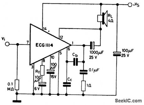
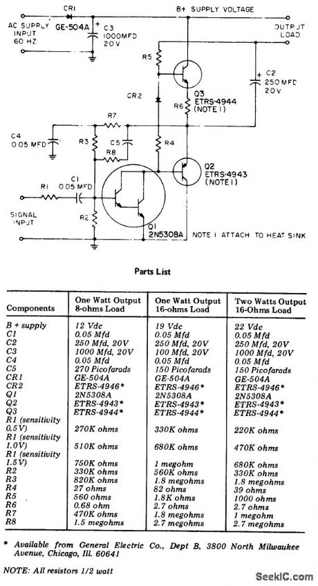
7_watt_AF_power_amplifier_featuring_thermal_shutdown_with_load_connected_to_the_supply_voltage
Published:2009/7/20 3:42:00 Author:Jessie
7-watt AF power amplifier featuring thermal shutdown with load connected to the supply voltage. Capacitor C3 is 1500 pF typically with C7 being 5600 pF. Generally C7 should be five times greater than C3. Typical supply voltage is 16 volts for the rated output. Input resistance is 5M. Input voltage is 220 mV PMS. With a supply voltage of 9 volts the output power will be 2.5 watts (courtesy GTE Sylvania Incorporated). (View)
View full Circuit Diagram | Comments | Reading(648)
33_watt_AF_power_amplifier_using_an_ECG1118_14_pin_QIP
Published:2009/7/20 4:33:00 Author:Jessie
3.3-watt AF power amplifier using an ECG1118 14-pin QIP. This circuit is designed for radio application (courtesy GTE Sylvania Incorporated). (View)
View full Circuit Diagram | Comments | Reading(690)
22_watt_AF_power_amplifiers_for_low_cost_phonographs_using_an_EGG1112_14_pin_DIP
Published:2009/7/20 2:56:00 Author:Jessie
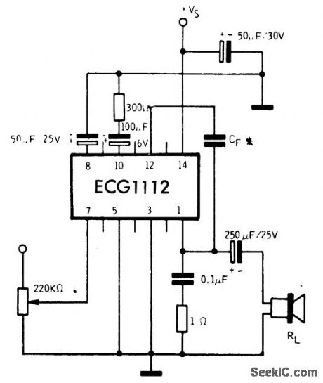
2.2-watt AF power amplifiers for low-cost phonographs using an EGG1112 14-pin DIP. The 2.2-watt rating is based on a 16-ohm load. Recommended supply voltage is 18 volts. Input impedance is 150K. Typical voltage gain is 72 dB. Current drain at maximum output is 175 mA. Capacitor OF can be either 510 pF or 820 pF. With OF at 820 pF the frequency response falls off at about 8 kHz; at 510 pF it extends up to 10 kHz (courtesy GTE Sylvania Incorporated). (View)
View full Circuit Diagram | Comments | Reading(705)
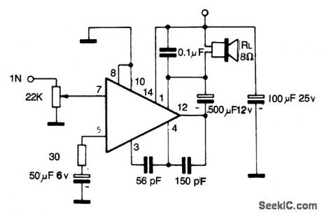
44_watt_audio_power_amplifier_for_a_4_ohm_load
Published:2009/7/20 2:55:00 Author:Jessie
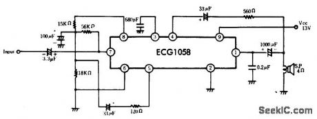
4.4-watt audio power amplifier for a 4-ohm load. The ECG1058 consists of a differential amplifier, a driver amplifier, a ripple filter, an automatic operating point stabilizer and a quasi-complementary SEPP OTL power amplifier circuit. This circuit is particularly good for automotive stereo applications since it is powered by a 13-volt supply. Typical voltage gain at 1 kHz is 45 dB (courtesy GTE Sylvania Incorporated). (View)
View full Circuit Diagram | Comments | Reading(806)
45_watt_AF_power_amplifier_with_grounded_load_for_radio_and_TV
Published:2009/7/20 3:41:00 Author:Jessie
4.5-watt AF power amplifier with grounded load for radio and TV. The ECG1114 is a 14-pin QIP. Current drain at maximum output is 485 mA. Typical voltage gain is 46 dB. Input impedance is 3M (courtesy GTE Sylvania Incorporated). (View)
View full Circuit Diagram | Comments | Reading(667)
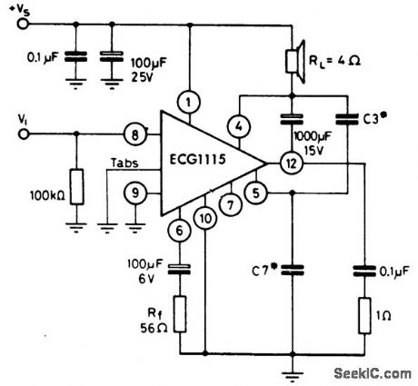
7_watt_AF_power_amplifier_featuring_thermal_shutdown_with_load_connected_to_ground
Published:2009/7/20 3:36:00 Author:Jessie
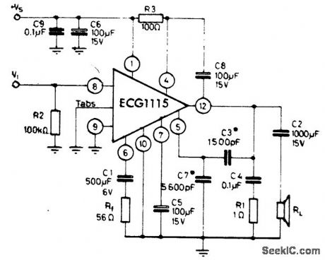
7-watt AF power amplifier featuring thermal shutdown with load connected to ground. For the rated output of 7 watts a 16-volt supply voltage is required. At a supply voltage of 9 volts the power output is 2.5 watts. Input voltage is 220 mV PMS. Input resistance is 5M. The ECG1115 is a 12-pin QIP with two metal tabs (courtesy GTE Sylvania Incorporated). (View)
View full Circuit Diagram | Comments | Reading(752)
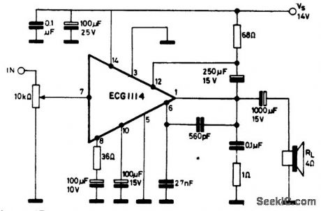
45_watt_AF_power_amplifier_for_radio_and_TV
Published:2009/7/20 3:35:00 Author:Jessie
4.5-watt AF power amplifier for radio and TV. Recommended supply voltage is 14 volts. Current drain at maximum power output is 485 mA. Typical voltage gain is 46 dB. Input impedance is 3M (courtesy GTE Sylvania Incorporated). (View)
View full Circuit Diagram | Comments | Reading(610)
25_watt_AF_power_amplifier
Published:2009/7/20 3:30:00 Author:Jessie
2.5-watt AF power amplifier. Recommended supply voltage is 17 volts. No-signal current is 24 mA. Input impedance is 85K (courtesy GTE Sylvania Incorporated). (View)
View full Circuit Diagram | Comments | Reading(618)
15_watt_2_watt_AF_power_amplifiers_using_an_ECG1141_1140_8_pin_DIP
Published:2009/7/20 3:29:00 Author:Jessie
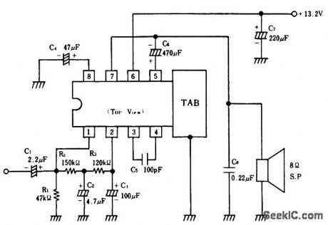
1.5-watt/2-watt AF power amplifiers using an ECG1141/1140 8-pin DIP. This amplifier is ideal for automotive applications since the recommended supply voltage is 13.2 volts. Typical voltage gain is between 51 and 56 dB. No signal supply current is 12 mA (courtesy GTE Sylvania Incorporated). (View)
View full Circuit Diagram | Comments | Reading(649)
High_gain_AF_preamplifier_using_an_ECG1135_7_pin_module
Published:2009/7/20 3:28:00 Author:Jessie
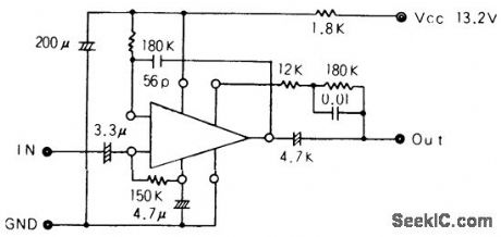
High-gain AF preamplifier using an ECG1135 7-pin module. This circuit is ideal for automotive stereo applications. No-signal supply current is 1.5 mA. Input impedance is 120K, while output impedance is 5 ohms (courtesy GTE Sylvania Incorporated). (View)
View full Circuit Diagram | Comments | Reading(615)
2_watt_AF_power_amplifier_with_bass_boost_for_a_16_ohm_load
Published:2009/7/20 3:25:00 Author:Jessie
2-watt AF power amplifier with bass boost for a 16-ohm load (courtesy General Electric Company). (View)
View full Circuit Diagram | Comments | Reading(747)
AF_preamplifier_with_a_thin_film_hybrid_module
Published:2009/7/20 3:22:00 Author:Jessie
AF preamplifier with a thin-film hybrid module. Output is between 0.42 and 0.90 volts at 1 kHz with a 2 mV input. Distortion is less than 3%. The AF transformer is standard and can be purchased at Radio Shack (courtesy GTE Sylvania Incorporated). (View)
View full Circuit Diagram | Comments | Reading(747)
| Pages:97/250 At 2081828384858687888990919293949596979899100Under 20 |
Circuit Categories
power supply circuit
Amplifier Circuit
Basic Circuit
LED and Light Circuit
Sensor Circuit
Signal Processing
Electrical Equipment Circuit
Control Circuit
Remote Control Circuit
A/D-D/A Converter Circuit
Audio Circuit
Measuring and Test Circuit
Communication Circuit
Computer-Related Circuit
555 Circuit
Automotive Circuit
Repairing Circuit