
Amplifier Circuit
Index 86
Norton_inverting_ac_amplifier
Published:2009/7/17 4:02:00 Author:Jessie
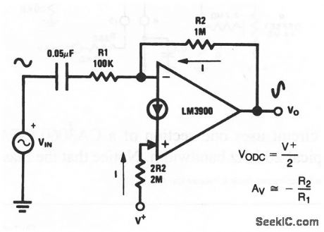
This circuit uses one section of an LM3900 to form an inverting ac amplifier with single-supply biasing (the circuit is biased from the same supply used to operate the amplifier). Figure 11-32B shows the pin connections for all four sections of an LM3900. If ripple voltages are present on the V+ power-supply line, the voltages will appear at the output with a gain of one-half. To eliminate this problem, one source of ripple-filtered voltage can be provided, and then used for many amplifiers, as shown in Fig. 11-33. National Semiconductor Linear Applications Handbook, 1991 p 218 220. (View)
View full Circuit Diagram | Comments | Reading(1088)
20_dB_amplifier
Published:2009/7/17 4:00:00 Author:Jessie
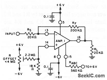
This circuit uses one section of a CA3060 OTA to form a 20-dB amplifier with a typical 20-kHz bandwidth.Notice that the bias input is connected to a fixed+6V. (View)
View full Circuit Diagram | Comments | Reading(1033)
Log_amplifier
Published:2009/7/17 3:54:00 Author:Jessie
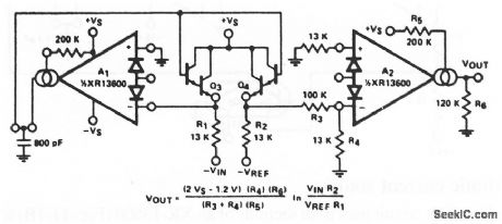
This circuit uses both sections of an XR-13600 (Fig. 11-1B) to form a log amplifier. The amplifier responds to the ratio of current through Q3/Q4. Zero temperature dependence for VOUT is ensured because the TC of the A2 transfer function is equal and opposite to the TC of the transistors. EXAR Corporation Databook 1990 p 5-258 (View)
View full Circuit Diagram | Comments | Reading(2374)
ADUSTABLE_CLOCK_FOR_MPU
Published:2009/7/10 23:46:00 Author:May
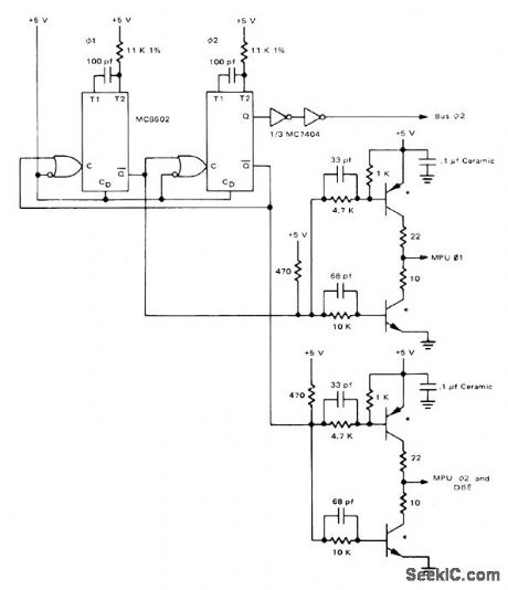
Two MC8602 cross-coupled mono MVBRs with individual pulse-width adjustments are used as clock oscillator to provide frequency flexibility for exnentation with data throughput,real-time operation with interrupts,and diagnosis of systiming problems,Required nonoverlapping clock pulses for phases 1 and 2 are generated by proagation delays through MVBRs,Transistors used for drivers are MPQ6842.- Microessor Applications Manual (Muturola Series in Solid-State Electronics), McGraw-Hill, New, York, NY, 1975, p 4-5—4-10. (View)
View full Circuit Diagram | Comments | Reading(696)
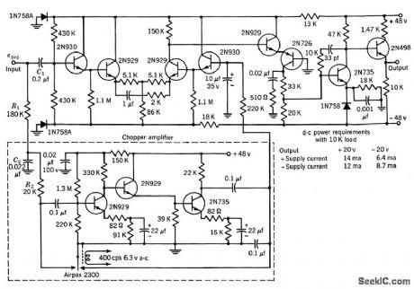
FET_AMPLIFIER_WITH_MECHANICAL_CHOPPER
Published:2009/7/10 23:44:00 Author:May
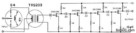
Gives readings down to10 nanovolls,with wideband response, because of remarkably low noise performance. Chopper frequency can be up to 1,500 cps.-Airpax Electronics (ad), Electronics, 39:15, p170. (View)
View full Circuit Diagram | Comments | Reading(1564)
AM_MODULATOR_LIMITING_AMPLIFIER
Published:2009/7/17 3:50:00 Author:Jessie
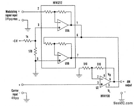
Limiting amplifiers also can be put to work in AM modulators. The fast overdrive recovery time and wide bandwidth of the clamp inputs allows these inputs to be driven by high-frequency ac, can as well as dc signals. When driven at the appropriate levels, the clamp inputs can be used to form an amplitude modulator. The HFA1130 limiting amplifier is driven by a 4-V p-p carrier signal. The gain of 2 through the HFA1130 ensures that the carrier amplitude is sufficient to drive the output over its±3.3-V range. The HFA1212 performs the necessary level shifting and inversion to convert the modulating signal input into a pair of antiphase signals that control the high and low clamp inputs. U1A inverts the signal and level-shifts to -1.5 V. U1B inverts that signal, forming a complementary signal centered at + 1.5 V. With a signal input of 0 V, U2 produces a 3-V p-p output at the carrier frequency. As the signal input varies, U2 produces a symmetrically modulated carrier with a maximum ampli-tude of6 V p-p. The 2300-V/μs slew rate of the HFA1130 limits 6-V p-p amplitude carrier signals to a frequency of 61 MHz. If adjusted for lower output-signal levels, the carrier and modulating frequencies can be increased to well above 100 MHz. (View)
View full Circuit Diagram | Comments | Reading(1765)
HALL_GENERATOR_CHOPPER_AMPLIFIER
Published:2009/7/10 23:36:00 Author:May
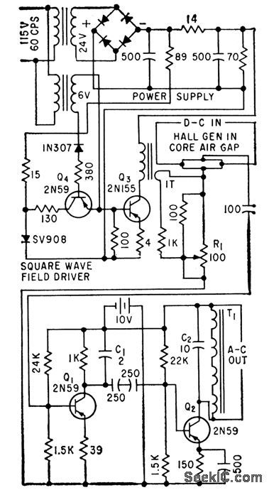
D-c signal voltage to be chopped is applied as control current of Hall generator. Magnetic field for generator is pulsed at 60 cps by driver circuit. Output is pulsating d-c voltage that is product of the two inputs. Error in input d-c versus output a-c is 2.5% for tem-perature range of -20 to 50℃. Can be used as d-c, a-c, or r-f microammeler.-T. J. Marcus, Highly Sensitive Electronic Chopper, Electronics, 32:40, p67-68. (View)
View full Circuit Diagram | Comments | Reading(728)
Ramp_and_hold
Published:2009/7/17 3:49:00 Author:Jessie
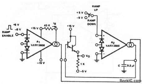
This circuit uses both sections of an XR-13600(Fig.11-1B). The circuit Sources IB into capacitor C whenever the input to A1 is made high,giving a ramp rate of about 1V/ms for the values shown.EXAR corporation Databook 1990 p 5-257 (View)
View full Circuit Diagram | Comments | Reading(844)
Peak_detector_and_hold
Published:2009/7/17 3:45:00 Author:Jessie
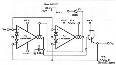


This circuit uses both sections of an XR-13600 (Fig. 11- 1B). The peak detector uses A2 to turn on A1 whenever VIN becomes more positive than VO. A1 then charges C to hold VO equal to VIN (peak). Notice that the Darlington used must be on the same side of the package as A2 because the Ay Darlington is turned on and off with A1. Pulling the output of A2 low through D1 serves to turn off A1 so that VO remains constant. EXAP Corporation Databook 1990 p 5 257 (View)
View full Circuit Diagram | Comments | Reading(934)
Sample_hold
Published:2009/7/17 3:44:00 Author:Jessie
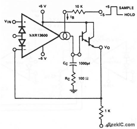
Although only one section is shown, this sample/hold circuit requires that the Darlington buffer be used from the other half of the package, and that the corresponding amplifier be biased on continuously. EXAR Corporation Databook, 1990, p 5-257. (View)
View full Circuit Diagram | Comments | Reading(766)
OP_AMP_VLF_RECEIVER
Published:2009/7/17 3:42:00 Author:Jessie
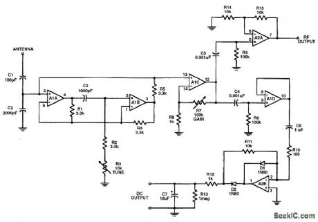
The figure shows the circuit diagram for an operational-amplifier VLF receiver. The circuit in the figure uses a virtual-inductor front end. A virtual inductor is a circuit that acts like an inductor, but isn't. Operational amplifiers AIA and AIB form a gyrator circuit. The inductance of this circuit is the product of the components shown between A1A and A1B [C3× 3300 × (R2 \+ R3)]. Capacitor C2 resonates with the virtual inductance produced by the gyrator circuit to tune the desired frequency. For the values of C2, CB, R2, and R3 shown, the circuit will tune from about 15 kHz to more than 30 kHz. Resistor R3 is the tuning control. It is a potentiometer, and should be either a multiturn knob via a vernier-reduction drive. The receiver front-end amplifier consists of amplifier A1C, which has a maximum gain of ×101 [i.e., (R7/R6)+1]. The output of A1C is an RF signal with a frequency equal to that tuned by the gyrator and C2. This signal is coupled to the RE output stage (A2A) through capacitor C5. The RF output stage shown here is a noninverting operational amplifier circuit with a gain of x2.The dc output circuit consists of a precise rectifier (A2B). The precise rectifier works like a regular rectifier, but does not have the low-voltage knee between 0 and 0.6 V (for silicon) or 0 and 0.2 V (for germanium). The pulsating dc from the precise rectifier is filtered and smoothed to straight dc, at a value proportional to the signal strength, by an RC integrator consisting of R12 and C7. The buffer amplifier (A1D) is used to isolate the precise rectifier from the RE output amplifier. (View)
View full Circuit Diagram | Comments | Reading(5243)
HYBRID_D_C_FEEDBACK_AMPLIFIER
Published:2009/7/10 23:14:00 Author:May
Used for calibrating a-c ammeters and voltmeters directly to standard cell.Use of tubes with chopper amplifier gives good temperature stability. Output to thermocouple is 7.5 ma.-E.A. Gilbert, Feedback Circuits for A-C Instrument Calibration,Electronics,33:40,p94-96 (View)
View full Circuit Diagram | Comments | Reading(700)
Schmitt_trigger
Published:2009/7/17 3:37:00 Author:Jessie
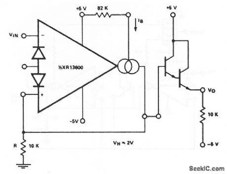
This circuit uses one section of an XR-13600 (Fig. 11-1B) to form a Schmitt trigger. The circuit uses the amplifier output current into R to set the hysteresis of the comparator, thus producing a variable hysteresis, where VH = 2×R×IB . EXAR Corporation Databook 1990, p 5-256 (View)
View full Circuit Diagram | Comments | Reading(0)
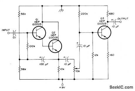
Servo_motor_preamplifier_3
Published:2009/7/17 3:35:00 Author:Jessie

Servo motor preamplifier (courtesy Motorola Semiconductor Products Inc.). (View)
View full Circuit Diagram | Comments | Reading(639)
Servo_motor_preamplifier_2
Published:2009/7/17 3:34:00 Author:Jessie
Servo motor preamplifier (courtesy Motorola Semiconductor Products Inc.). (View)
View full Circuit Diagram | Comments | Reading(709)
Phase_locked_loop
Published:2009/7/17 3:34:00 Author:Jessie
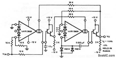
This PLL uses the four- quadrant multiplier (Fig. 11-4) and VCO (Fig.11-16).The circuit has a ±5% hold- in range and an input sensitivity of about 300 mV EXAS corporation Databook 1990 p 5-256 (View)
View full Circuit Diagram | Comments | Reading(0)
TELEPHONE_AMPLIFIER
Published:2009/7/10 23:11:00 Author:May
This amplifier can be used in telephone work or where a simple speech amplifter is required. The frequency response can be varied by the value of C2. C4. and addition of a capacitor across R4 ( ≈ 33 pF for voice band) to limit the HF response. (View)
View full Circuit Diagram | Comments | Reading(0)
CHOPPER_STABILIZED_D_C_OPERATIONAL_AM_PLlFlER
Published:2009/7/10 22:44:00 Author:May
Mechanicctl chopper amplifier amplifies low-level d-c portion of input signal, for further amplilcation by stages that also am plify superimposed a-c information. Circuit has excellent d-c stability and wide band-width. D-c gain is l20 db and gain at 10 kc is 45 db.-Texas Inslruments Inc. Iron-sistor Circuit Design, McGraw-Hill, N.Y.1963,p195. (View)
View full Circuit Diagram | Comments | Reading(817)
HIGH_Z_CRO_PREAMP
Published:2009/7/10 22:39:00 Author:May
Darlington circuit provides extremely high input impedance (over 2.2 megohms). With input shorted, noise level is 78 dB down as read at output whh VTVM. Linearity is within 1.5% for inputs from 100 μV to 1 mV, and frequency response is ±2 dB from 100 Hz to 350 kHz. Originally designed to boost input to CRO, but can be adapted to many other applications requiring high gain, low noise, and high input impedance.-J. Fisk, Circuits and Techniques, Ham Radio, June 1976, p 48-52. (View)
View full Circuit Diagram | Comments | Reading(805)
TEMPERAIURE_TO_FREOUENCY__CONVERTER
Published:2009/7/10 22:38:00 Author:May
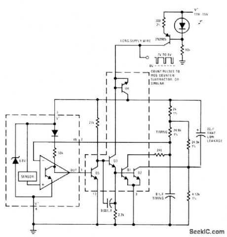
Transistors Q1-Q5 in National LM3046 transistor array form oscillator and ramp that together convert varying output voltages of LX5600 temperature transducer to poportional changes in frequency of squatevwave pulses for feed to pulse counter.-P Lefferts, A New Interfacing Concept;the Monolithic TemperatureTransducer, National Semiconductor, Santa Clara,CA,1975,AN-132,p 4. (View)
View full Circuit Diagram | Comments | Reading(647)
| Pages:86/250 At 2081828384858687888990919293949596979899100Under 20 |
Circuit Categories
power supply circuit
Amplifier Circuit
Basic Circuit
LED and Light Circuit
Sensor Circuit
Signal Processing
Electrical Equipment Circuit
Control Circuit
Remote Control Circuit
A/D-D/A Converter Circuit
Audio Circuit
Measuring and Test Circuit
Communication Circuit
Computer-Related Circuit
555 Circuit
Automotive Circuit
Repairing Circuit