
Amplifier Circuit
Index 80
WIDER_BANDWIDTH_PHOTODIODE_AMPLIFIER
Published:2009/7/13 2:03:00 Author:May
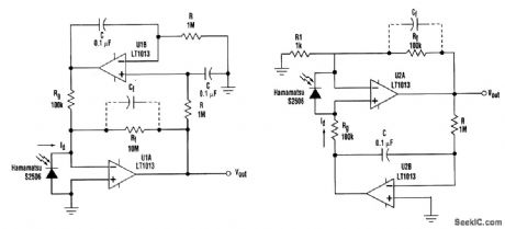
Many photodiode applications require high gain and wide bandwidth. A dc-restored photodiode amplifier (Fig. 1) is useful in situations where a time-varying light signal of interest competes with unwanted ambient background light. To extend the amplifier's bandwidth, the design can be modified to provide current-to-voltage conversion with subsequent voltage gain (Fig. 2). Current from the low-capacitance photodiode flows through Rg and establishes a voltage at the noninverting terminal. This voltage then receives a gain equal to 11Rf/R1. With the values shown in Fig. 2, the equivalent transimpedance Rg(11Rf/R1) is equal to 10Ω. The design uses an invertingintegrator to drive a restoration current through Rg This low-frequency current cancels current from the photodiode at frequencies below the low-frequency cutoff pole. The low-frequency pole in Fig. 2 is given by f-3dB5 (1/2πRC) (11Rf/R1). For the values shown, this is equal to 159 Hz. Rg helps determine the equivalent transimpedance and provides the path for the low-frequency restoration current. The measured high-frequency cutoff for the circuit in Fig. 1 is 4.9 kHz, with a total in-bartd noise of 370 μV rms. In Fig. 2, the high-frequency cutoff is extended to 11.7 kHz, with a total in-band noise of 589 μV rms.
(View)
View full Circuit Diagram | Comments | Reading(3810)
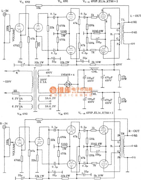
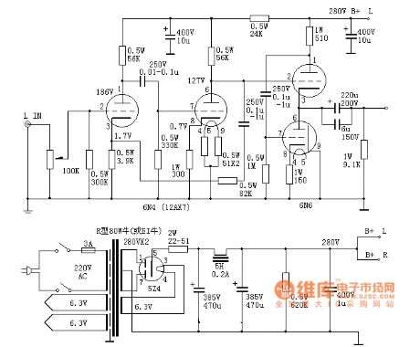
Tube stereo power amplifier circuit diagram
Published:2011/8/4 1:33:00 Author:Ecco | Keyword: Tube stereo, power amplifier
View full Circuit Diagram | Comments | Reading(1271)
DIFFERENTIAL_AMPLIFIER
Published:2009/7/13 1:56:00 Author:May
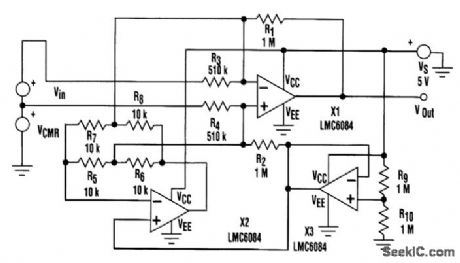
The differential amplifier shown handles common-mode voltages up to ±24 V on a 3.3-V supply, or up to ±40 V on a 5-V supply. It is handy when interfacing analog-to-digital converters (ADCs) or data-acquisition systems (DASs) in 3.3-V or 5-V single-supply systems to inputs with a wide common-mode range. Differential amplifier X1 is the actual differential amplifier, and R1, R2, R3, and R4 are the gain-setting resistors. X2 forces the common-mode voltage at X1's inputs to zero with respect to a quiescent biasing point provided by X3. The wide availability of dual and quad low-voltage op amps permits implementations with a single IC package. Biasing at one-half supply, or at some reference well within the supply rails, is necessary because positive-going common-mode inputs require X2's output to swing negative. R5, R6, R7, and R8 should have impedance at least an order of magnitude less than the gain-setting resistors of X1. The impedance relationship of R6 and R8 to gain-setting resistors limits the use of this circuit to high-impedance differential-amplifier circuits. Therefore, it is not well suited for wide-bandwidth circuits. The high impedances also favor the use of JFET or CMOS input op amps. (View)
View full Circuit Diagram | Comments | Reading(0)
Integrated audio amplifier circuit diagram
Published:2011/8/4 1:28:00 Author:Ecco | Keyword: Integrated audio amplifier
View full Circuit Diagram | Comments | Reading(1012)
ACCURATE_LOG_AMPLIFIER
Published:2009/7/13 1:54:00 Author:May
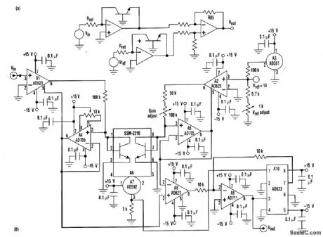
The log circuit consists of an instrumentation amp and an Op amp together with a diode-connectedtransistor that produces a voltage proportional to the logarithm of the current A circuit consisting of avoltage reference, an instrumentation amp,and an op amp,togetherwith a diode-connected transistor,acts as a reference circuit. A thermometer IC,a fixed-gain instrumentation amp,and a divider circuitprovide the necessary temperature compensation and scaling for a transfer function∶Vout51.985 log10 (Vin/1V)Vref must be set to 1.000 V and, with Vin 5Vref, the gain adjust has to be set so that VO 50 V. Calirelbration low input voltage is done by changing buffer A4's offset voltage. (View)
View full Circuit Diagram | Comments | Reading(2517)
WIDEBAND_CURRENT_FEEDBACK_AMPLIFIER
Published:2009/7/13 1:45:00 Author:May
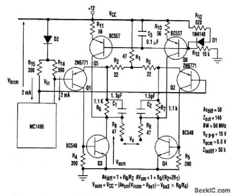
When using multipliers such as the LM1496 or MC1496, low-value output resistors are necessary to obtain maximum bandwidth. This reduces the output swing available, which necessitates a differ-ential high-gain, wideband amplifier. The amplifier has a differential gain (AV,diff) of 50 and a band-width of about 50 MHz, giving it a total gain-bandwidth product of 2.5 GHz. It also provides an output swing of 18 V p-p from a 112-V supply. Transistors Q1 and Q2 form a differential pair that drives Q3 and Q4. Feedback is provided to the emitters of Q1 and Q2 by R6, C1 and R7, C2, which bootstraps the input impedance and sets the overall gain. Q5 and Q6 provide about 15 mA of current each, pro-viding most of the sourcing current for the load. The basic design equations are provided to modify component values to suit different applications.Simply envision the circuit is as a differential current-feedback amplifier, with the low-imped-ance port being the emitters of Q1 and Q2, and the current output as the collectors of Q3 and Q4.Because the output is a bridge circuit and the maximum positive current is set by R6, R7 and Q5, Q6, the output is short-circuit-protected between resistors R8 and R9. RI can be replaced by a current source to reduce the common-mode gain. The main criterion is to balance the currents at the emit-ters of Q1 and Q2 to give a common-mode output voltage of VCC/2. Some care should be taken when driving capacitive load because the circuit can oscillate under such conditions. (View)
View full Circuit Diagram | Comments | Reading(2025)
ORYSTAL_RADIO_AMPLIFIER
Published:2009/7/13 1:43:00 Author:May
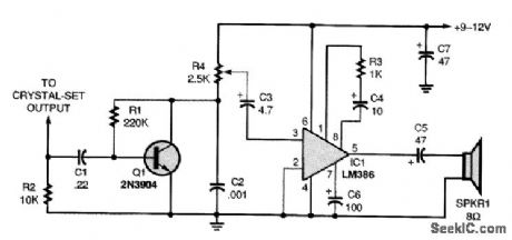
If you'd like to hear your crystal set at a comfortable, room-filling volume, hook it up to this amplifier. (View)
View full Circuit Diagram | Comments | Reading(996)
ELECTRET_MIKE_PREAMP_WITH_PTT_CIRCUIT
Published:2009/7/13 1:41:00 Author:May
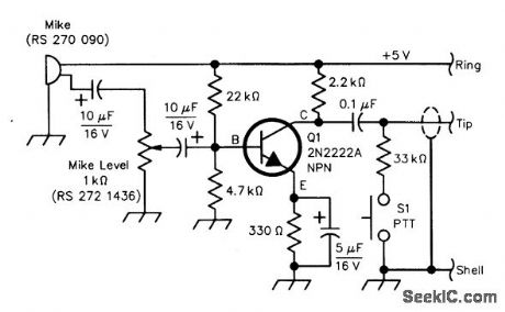
The schematic of electret mike element and amplifier circuit All resistors are 1/4-W units. The mike connector is an RS 274-284. (View)
View full Circuit Diagram | Comments | Reading(2004)
LIGHT_PEN_AMPLIFIER
Published:2009/7/16 20:39:00 Author:Jessie
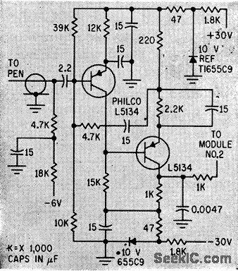
Consists of four two-transistor wideband-amplifier modules, each withinverse feedback to hold current gain at 21 with high stability.Interstage coupling networks raise lower cutoff frequency to 500 cps, to provede some rejection of 120-cps room light picked up by photodiode.-B.M. Gurley and C.E.Woodward,Light-Pen Links Computer to Operator,Electronics,32:47,p 85-87. (View)
View full Circuit Diagram | Comments | Reading(876)
HIGH_GAIN_AMPLIFIER
Published:2009/7/13 1:34:00 Author:May
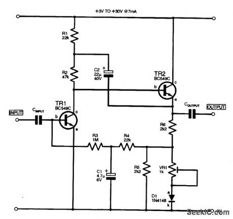
This high-gain inverting amplifier stage was designed to operate with a rail of between 3 and 30 V. It includes a bootstrap network (R1, C2), which serves to increase the gain of the stage to approximately 3000, as well as offering a low-distortion output waveform at maximum amplitudes. The input impedance is approximately 80 kV at 200 Hz, the output level is 80 percent at 20 kHz, and noise at the output is 14 mV p-p. R5 and D1 were included to proportionately lower the bias to TR1 to compensate for any increases in the rail voltage; R5 can be omitted and Dl shorted out if the rail is con-stant. VR1 is adjusted to give symmetrical clipping of the maximum output signal.
(View)
View full Circuit Diagram | Comments | Reading(2063)
380MHz linear amplifier circuit composed of RF2175
Published:2011/8/4 3:18:00 Author:May | Keyword: linear amplifier, 380MHz
Radio-frequency signal ( RF) is input by pin 6 andoutput by pin 12, 13 after being enlarged by preamplifier, final amplifier. Pin 6 is directly coupled with inside amplifier, so we must add a blocking coupling capacitor. Pin 12 and 13 are used as the final stage power amplifier power supply end, which can provide bias current for the final amplifier. pin 14 is used as the second harmonic filter circuit, which uses the transmission lines or inductor and capacitor to form filter with resonance in 2f0, and it can provide low impedance path for the second harmonic, which can effectively short the second harmonic. (View)
View full Circuit Diagram | Comments | Reading(863)
432_MHz_PREAMP
Published:2009/7/16 6:59:00 Author:Jessie
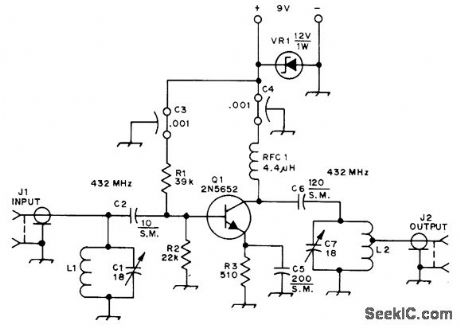
Developed as part of 400-MHz radiotelescope, for low-noise operation. Gain is 12 dB, and noise figure is below 2 dB. Circuit is basic common-emitter amplifier with tuned input and output. Neither neutralization nor shielding are needed. Supply can be 9-V transistor radio battery. Current drain is 3mA. L1 and L2 are each 1 turn No. 16 wire3/8 inch in diameter, with L2 center-tapped.-S. A, Maas, An Inexpensive Low Noise Preamplifier for 432 MHz, QST, Jan. 1975, p 21-22. (View)
View full Circuit Diagram | Comments | Reading(1959)
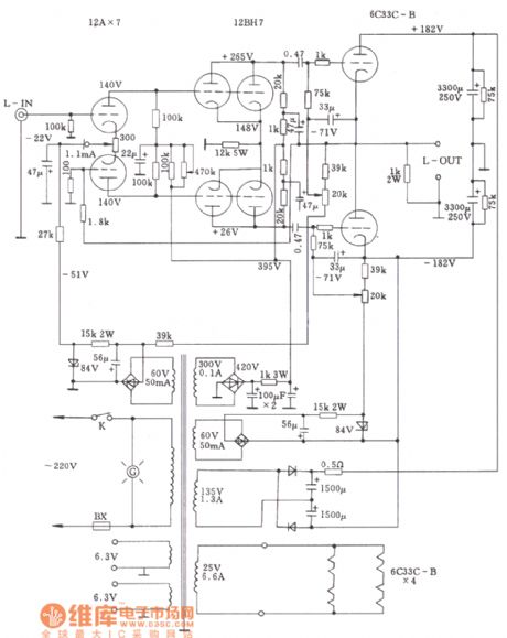
Vacuum tube headphone amplifier circuit diagram
Published:2011/8/3 21:44:00 Author:Ecco | Keyword: Vacuum tube, headphone amplifier
View full Circuit Diagram | Comments | Reading(3639)
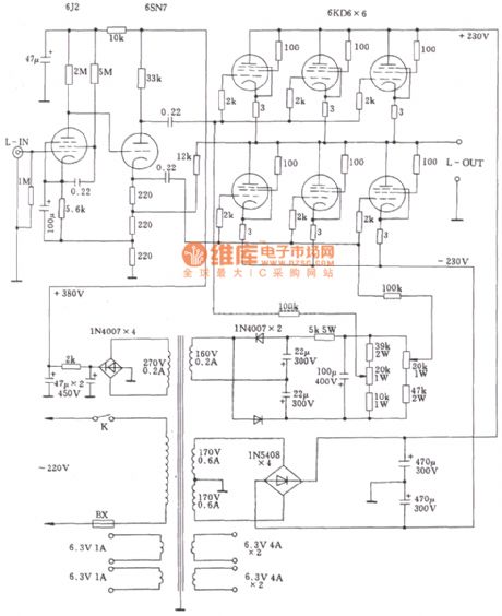
New three-pole power tube OTL power amplifier circuit diagram
Published:2011/8/3 21:43:00 Author:Ecco | Keyword: New three-pole , power tube OTL , power amplifier
The frequency of the machine can be 10Hz to 200KHz at ±0.1dB. Each sound track's power can reach 40w at 8Ω load.
(View)
View full Circuit Diagram | Comments | Reading(2118)
HEADPHONE_AMPLIFIER_FOR_GUITARS
Published:2009/7/12 23:45:00 Author:May
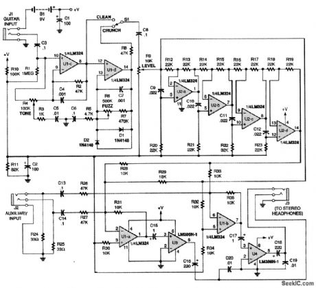
From the hard distortion provided by U1-d and D1 and D2 to the stereo imaging accomplished by U2, this is a guitarist's dream come true. Note that there is no power switch in the circuit; J1 turns on the unit whenever an instrument cable is plugged in.The main components in the circuit are two LM324 quad op amp ICs (U1 and U2) and two LM386 power amp ICs (U3 and U4). The inputs to U1 and U2 are biased to a little less than half the power-supply voltage by resistors R10 and R11. Capacitors C1 and C2 filter the power-supply and bias voltages. J1 turns on the amplifier when the input plug is inserted. When an audio signal from an instrument is input through J1, the signal is fed through coupling capacitor C3 to the tone-controlcircuit composed of U1-c, R2, R4, and C4. Frequencies above 1 kHz are amplified or attenuated depending on the position of potentiometer R4, which is the tone control. Resistor R2 and capacitor C4 filter unwanted high frequencies. Audio level and overdrive are controlled by potentiometer R9; with that level control adjusted to full volume, the circuit's final amplifiers are overdriven to produce a soft distortion effect. To prevent any unwanted dc swishing noise, a coupling capacitor, C8, is used.Switch S1 toggles between the clean and distorted signals. When S1 is on the CRUNCH setting, diodes D1 and D2 and U1-d produce a distortion effect by clipping the amplified signal at 0.7 V. Frequencies below 160 Hz are attenuated by R5 and C6. The amount of gain or fuzz is controlled by R7 and potentiometer R6, and resistor R8 adjusts the distortion level to match the tone-control level.
(View)
View full Circuit Diagram | Comments | Reading(1659)
New five-pole power tube OTL power amplifier circuit diagram
Published:2011/8/3 21:41:00 Author:Ecco | Keyword: New five-pole , power tube OTL , power amplifier

The output power can reach 50W at the 8Ω load.
(View)
View full Circuit Diagram | Comments | Reading(2266)
The 0TL power amplifier connection circuit diagram of Ordinary power tube changing into triode
Published:2011/8/3 22:30:00 Author:Ecco | Keyword: 0TL , power amplifier connection , Ordinary power tube , triode
View full Circuit Diagram | Comments | Reading(1220)
2_W_STEREO_AMPLIFIER
Published:2009/7/12 23:42:00 Author:May
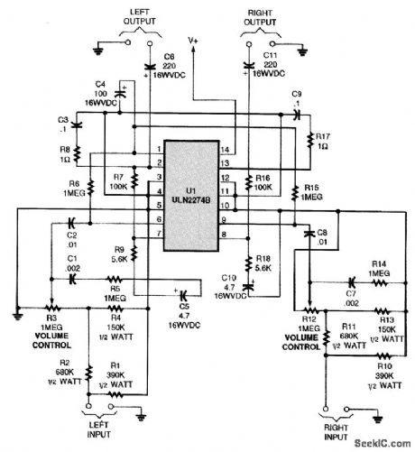
The amplifier is built around a ULN2274B dual audio power amplifier and provides a maxintum of 2 W of quality sound. Because the amplifier is composed of two identical subcircuits, only one subcircuit will be covered. Resistor R5 sets the tone and it can be replaced with a variable unit; lower values of that resistor produce more bass. The bias is set by R6 and C4, and R7, R9, and C5 are feedback elements. For a more realistic sound, R8 and C3 are used to roll off the high frequencies. Capacitor C6 is a dc-blocking capacitor. The circuit chip requires from 6 to 26 Vdc without distortion.
(View)
View full Circuit Diagram | Comments | Reading(888)
PROGRAM_TIMER
Published:2009/7/12 23:41:00 Author:May
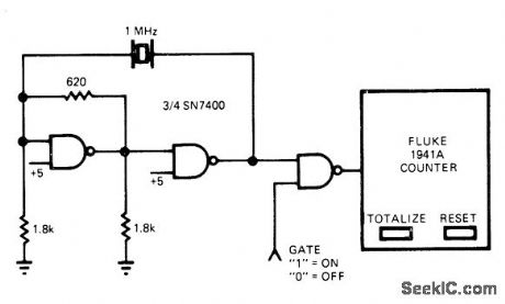
Measures time between two points in microprocessor program while program is running. Gated 1-MHz crystal oscillator feeds Fluke 1941A counter used in totalize mode. Gate input is connected to unused bit of output port on microprocessor system. Instruetions are then inserted in program under test to gate counter on at beginning of desired step and turn it off at end. I)isplay then shows number of microseconds required by microprocessor to execute instructions.-M. M. Dodd, Benchmark Timer Eliminates Need to Total Individual Execution Times, EDNMagazine, Oct.20,1975,p91-92. (View)
View full Circuit Diagram | Comments | Reading(1031)
SIMPLE_AUDIO_OUTPUT_AMPLIFIER
Published:2009/7/12 23:39:00 Author:May
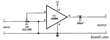
This audio amplifier circuit has a gain of about 20. A supply of 3 to 12 V cart be used. Output is up to about 1 W, depending on load impedance and supply voltage. (View)
View full Circuit Diagram | Comments | Reading(842)
| Pages:80/250 At 206162636465666768697071727374757677787980Under 20 |
Circuit Categories
power supply circuit
Amplifier Circuit
Basic Circuit
LED and Light Circuit
Sensor Circuit
Signal Processing
Electrical Equipment Circuit
Control Circuit
Remote Control Circuit
A/D-D/A Converter Circuit
Audio Circuit
Measuring and Test Circuit
Communication Circuit
Computer-Related Circuit
555 Circuit
Automotive Circuit
Repairing Circuit