
Amplifier Circuit
Index 62
LM4808 Dual-channel headphone amplifier circuit diagram
Published:2011/8/22 22:21:00 Author:Rebekka | Keyword: Dual-channel headphone amplifier
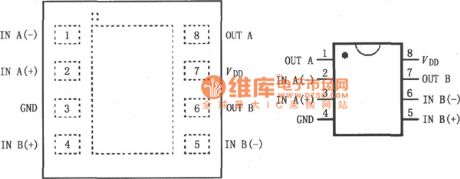
LM4808 is a dual-channel headphone amplifier. It uses 5V power supply. The average power of each channel is output 105mW. It drives 16Ω load. Total harmonic distortion and noise(THD+N) are 0.1% only. LM4808 Audio power uses surface pakage. It has a minimum number of external component. It provides high-quality output power. LM4808 does not require bootstrap capacitors and buffers. So it is the best suitable one for low-power portable systems. It has a stable overall gain. It can be set by external gain resistors. LM4808 can be used for headphone amplifier, personal computer and portable electronic devices. (View)
View full Circuit Diagram | Comments | Reading(1313)
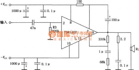
TDA1102 20WHi-Fi Power amplifier circuit diagram
Published:2011/8/22 22:14:00 Author:Rebekka | Keyword: 20WHi-Fi, Power amplifier
View full Circuit Diagram | Comments | Reading(1439)
Op amp power supply decoupling bypassing measure circuit diagram
Published:2011/8/22 22:12:00 Author:Rebekka | Keyword: Op amp power supply, decoupling bypassing measure
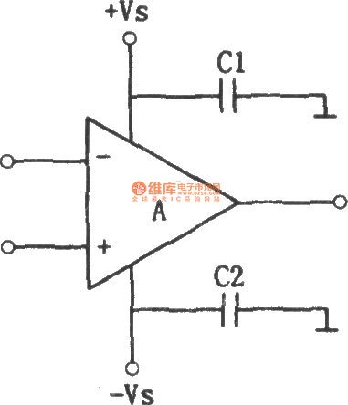
Each power lead of the integrated power amplifier generally uses decoupling bypassing measure. That means connecting a high-performance capacitor from power lead end to extend across. It is shown in the figure. The high frequency bypass capacitor shown in the figure usually chooses a high performance ceramic capacitor, its value is 0.1μF. It can also use lμF tantalum capacitor. The internal inductance of these capacitors are small. When the op amp works in a high-speed, the bypass capacitors C1 and C2 should be connected to the power supply pins of integrated amplifier. The leads should be as short as possible to form a low inductance ground return circuit. When the gain-bandwidth of the used amplifier is greater than 10MHz, you should adopt more stringent high-frequency bypass measures. (View)
View full Circuit Diagram | Comments | Reading(3275)
Op amp input compensation capacitor circuit diagram
Published:2011/8/22 22:12:00 Author:Rebekka | Keyword: Op amp, input compensation capacitor
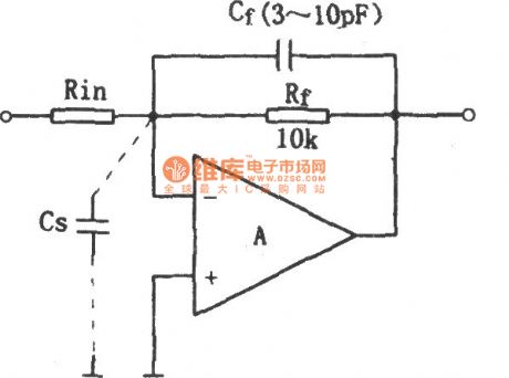
General linear amplifier (namely the work of the negative feedback amplifier circuit) input parasitic capacitance will influence the stability of Cs circuit, the compensation measures are shown in the map. The amplifier's input generally exists a few parasitic capacitance Cs. The Cs includes op-amp input capacitance and wiring distributed capacitance. Its feedback resistor Rf can form a lag network and cause output voltage phase lag. When the input signal frequency is high, the bypass action of the Cs makes the amplifier's high frequency response become worse, the frequency band of the upper limit of frequency is about: Omega h = 1 / (2 PI RfCs) . (View)
View full Circuit Diagram | Comments | Reading(4834)
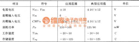
Basic inverting amplifier circuit composed of the μA709
Published:2011/8/22 22:10:00 Author:Rebekka | Keyword: Basic inverting amplifier
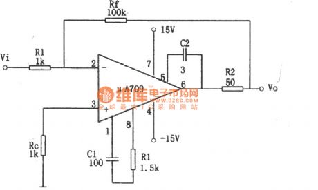
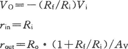
The figure of the basic inverting amplifier circuit composed of the μA709 is shown as above.
The main performance of the U A709 :
According to the figure, the feedback resistor Rf will connect the output and input ends. Since the circuit output, input voltage are inverting, the Rf leads the voltage parallel negative feedback. Thereby the amplifier works in linear region with the op-amp transmission characteristics, that is, the output voltage is proportional to the input voltage. In addition, the inverting input end is connected to the resistor Ri in series, and it is the operational amplifier's input resistor. The increasing of Ri can reduce the source of the load.
(View)
View full Circuit Diagram | Comments | Reading(1123)
High-speed programmable gain amplifier circuit composed of the INA110
Published:2011/8/12 4:23:00 Author:Rebekka | Keyword: High-speed , programmable gain amplifier

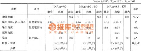
The figure shows the high-speed programmable gain amplifier circuit. The main circuit is composed of the rapid and stable instrument integration op-amp INA110. Because the INA110 builds time fast, so it is the ideal amplifier circuit for the high speed or multiple data acquisition system. When the gain Av = 100, its build time can be up to 3 us.
(View)
View full Circuit Diagram | Comments | Reading(1180)
M51304L Microphone amplifier circuit diagram
Published:2011/8/12 4:20:00 Author:Rebekka | Keyword: Microphone amplifier
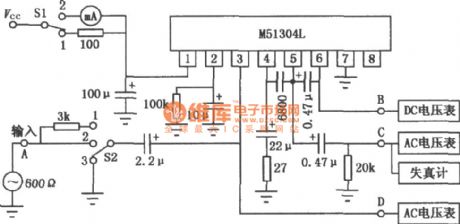
M51304L is microphone amplifier circuit. It uses 8-pin single inline package. The power supply voltage is 8~15V with low noise. There is automatic gain control (AGC) circuit inside. You can adjust the sensitivity of agc though external resistor. It is suitable for the microphone amplifier of micro recorder. The typical application circuit diagram is shown as below.
(View)
View full Circuit Diagram | Comments | Reading(2625)
LLC-KING AB class amplifier circuit diagram
Published:2011/8/24 1:49:00 Author:Ecco | Keyword: LLC-KING , AB class amplifier
View full Circuit Diagram | Comments | Reading(1004)
Actin voltage amplifier circuit diagram
Published:2011/8/12 3:20:00 Author:Lucas | Keyword: Actin voltage amplifier

This circuit is used to enlarge a few millivolts of 20 ~ 5000HZ signal voltage. This signal is picked up by putting the 13mm thin silver film on human skin. When people do ECG measurements, each wrist should be put one electrode, the source impedance is up to 50kΩ. The maximum output capacity of the circuit is 9Vp-p voltage. The voltage gain is 1000. RF is the 800K potentiometer to adjust the frequency be higher crossover frequency, then the octave is shut down 12dB.
(View)
View full Circuit Diagram | Comments | Reading(1536)
Voltage regulator DC-DC circuit and power supply monitor pins introduction and main features TA8002S constant voltage regulator
Published:2011/8/17 20:12:00 Author: | Keyword: Voltage regulator, power supply monitor, pins introduction, main features, constant voltage regulator
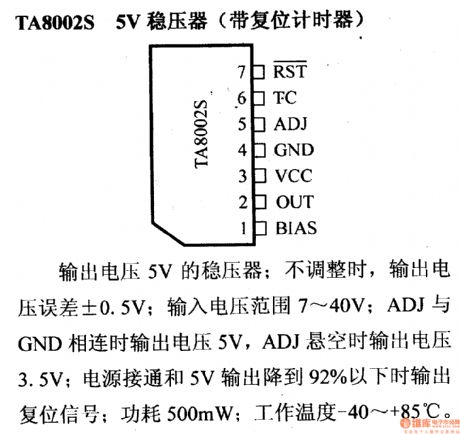
TA8002S constant voltage regulator Its output voltage is 5 V with a difference of +/- 0.5 V. And its voltage coverage is from 7 V to 40 V. When ADJ is connected to GND, its output voltage is 5 V and when ADJ is suspended in midair, the output voltage is 3.5 V. It outputs restart signal when the power supply is connected and output voltage of 5 V lowers to 92% with the power consumption of 500mW. Its operating temperature is -40oC to +85oC. (View)
View full Circuit Diagram | Comments | Reading(770)
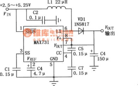
MAX731 switch control DC-DC boosting convertor
Published:2011/8/11 11:25:00 Author:leo | Keyword: Switch, DC-DC boosting convertor
View full Circuit Diagram | Comments | Reading(680)
The classic applying circuit of MAX752 setting up switch DC-DC convertor
Published:2011/8/14 7:19:00 Author:leo | Keyword: Classic applying circuit, setting up switch, DC-DC convertor
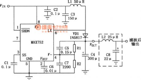
View full Circuit Diagram | Comments | Reading(654)
2SK134/J49 Power amplifier circuit diagram
Published:2011/8/11 2:17:00 Author:Rebekka | Keyword: Power amplifier
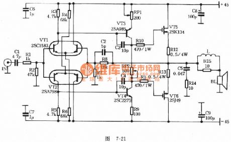
Resistor uses the1/2W high quality metal film resistor. The capacitor uses the imported CBB capacitor. All the transistors must be matched strictly. Matching error must be controlled in 3%. L uses the 1.0mm enameled wire with 10 turns tightly wound on 12mm frame. You can adjust the quiescent currentaround 100mA afterpower amplifier tube welding correctly andcheck the matching transistor error if midpoint potential of the circuit can not be controlled under 30mV.
(View)
View full Circuit Diagram | Comments | Reading(5331)
AT-HA2002 Headphone amplifier copy diagram
Published:2011/8/9 2:25:00 Author:Rebekka | Keyword: Headphone amplifier, copy diagram
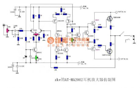
AT-HA2002 Headphone amplifier copy diagram is shown as below.
(View)
View full Circuit Diagram | Comments | Reading(2248)
6P6P Headphone amplifier circuit diagram
Published:2011/8/11 2:18:00 Author:Rebekka | Keyword: Headphone amplifier
View full Circuit Diagram | Comments | Reading(694)
The differential input and differential output amplifying circuit composed of the INA102
Published:2011/8/11 2:37:00 Author:Rebekka | Keyword: differential input , differential output , amplifying circuit
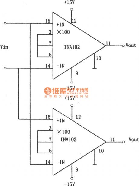
The figure shows the differential input differential output amplification circuit. In some applications, the signal source and the output voltage are not allowed to grounding, at this time, it should use the differential input and output, this circuit differential way can be composed by the INA102 and INA105. The figure shows the circuit comosed of the INA102, andthis kind of amplifier circuit does not need external components. Each INA102 voltage magnification factor is l00, ifit has different phase (voltage amplifier magnification factoris negative and positive), the general voltage amplifier magnification factor is 200. The total output voltage Vo = 200 Vi. (View)
View full Circuit Diagram | Comments | Reading(851)
Broadband differential input / differential output amplifier circuit diagram composed of OPA606
Published:2011/8/11 2:29:00 Author:Rebekka | Keyword: Broadband , differential input, differential output , amplifier
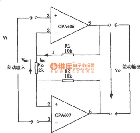
When the input / output signals are not allowed to ground and they need a wide pass band, the icon broadband differential input / differential output amplifier can be used. In the figure, the circuit uses two types of broadband FET input operational amplifiers OPA606. The device uses the dielectric isolation process, so the op amp is used as Difet op amp. The device has a high input impedance and low input bias current, in addition, OPA606 op amp circuit uses laser trimming technology, thus OPA606 has the features of low offset voltage and low noise.
(View)
View full Circuit Diagram | Comments | Reading(1516)
The differential amplifier with low-pass filtering circuit composed of the OPA2604
Published:2011/8/11 2:31:00 Author:Rebekka | Keyword: differential amplifier , low-pass filtering
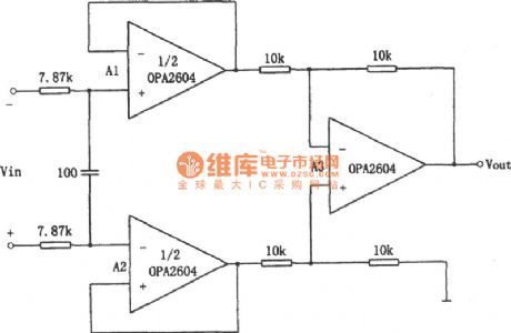
The figure shows a low pass filtering differential amplifier circuit. This circuit has the 100 Hz ac low pass filtering, differential input, single-end outputand high fidelity. The OPA2604 amplifier circuit is the mosfet inputdual op-amp integrated circuit. The OPA2604 is connected into two voltage follower. It is shown in figure A1, A2. Because OPA2604 has a very high input impedance (1012 Ω / / 8 pF) and a very low offset current (50 pA), therefore it can ensure the circuit has good filtering effect. The OPA604 is single op-amp and OPA2604 is double op-amp. Both characteristics are completely the same.
(View)
View full Circuit Diagram | Comments | Reading(1857)
LM3886 Subwoofer circuit diagram
Published:2011/8/9 2:24:00 Author:Rebekka | Keyword: Subwoofer
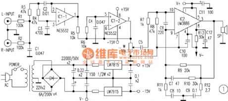
View full Circuit Diagram | Comments | Reading(4256)
The piezo-electric transducer using high-impedance high-fidelity amplifier circuit diagram
Published:2011/8/11 2:12:00 Author:Rebekka | Keyword: piezo-electric transducer , high-impedance high-fidelity amplifier

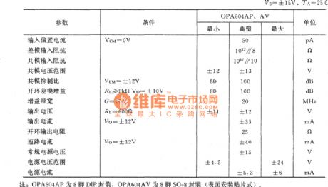
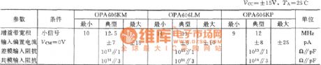
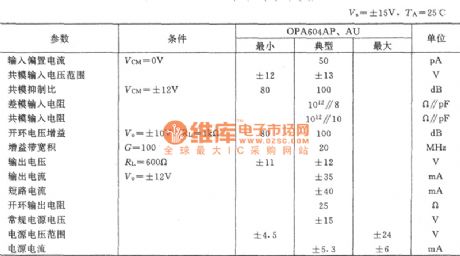
The main parameters of the OPA604:
In the automatic control system or some detection system, the sensor piezoelectric devices is often used as sensor. So as to realize the power electrical signals. This kind of sensor equivalent sources has very high resistance and the signal is very weak. So it must also be matching high input impedance amplifier circuit, and the amplify circuit must also have the ability to accurately weaken signal amplifier. The figure gives high fidelity op-amp OPA604 constitute amplifier circuit.
(View)
View full Circuit Diagram | Comments | Reading(1454)
| Pages:62/250 At 206162636465666768697071727374757677787980Under 20 |
Circuit Categories
power supply circuit
Amplifier Circuit
Basic Circuit
LED and Light Circuit
Sensor Circuit
Signal Processing
Electrical Equipment Circuit
Control Circuit
Remote Control Circuit
A/D-D/A Converter Circuit
Audio Circuit
Measuring and Test Circuit
Communication Circuit
Computer-Related Circuit
555 Circuit
Automotive Circuit
Repairing Circuit