
Amplifier Circuit
Index 60
The RF wide band amplifier unit circuit of separated elements
Published:2011/8/23 22:13:00 Author:Borg | Keyword: wide band amplifier, separated elements
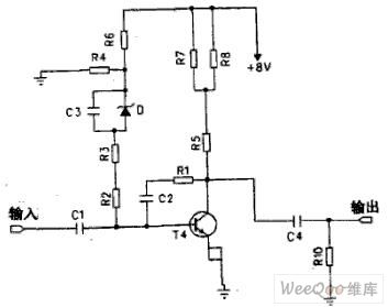
The RF wide band amplifier unit circuit of separated elements is shown as above.
(View)
View full Circuit Diagram | Comments | Reading(1345)
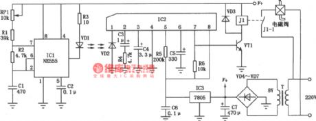
The self-made independent element 50W hi-fi power amplifier circuit
Published:2011/8/23 22:13:00 Author:Borg | Keyword: independent element, hi-fi, power amplifier
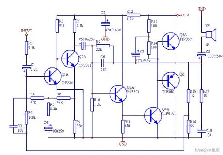
The power amplifier stage of the amplifier circuit consists of the compensatory tube emitter follower, the backward feedback of the big circuit makes the drive compensatory tube signal in the linear range. The circuit makes sure the 2 tubes conduct in different time in the structure, so the power supply won't be short.
Ideal transistors can conduct or block quickly, however, triodes switch speed is limited, not to say the large power tube. When the changing signal which is put in the tube is reversed, the 2 tubes may be conducting at the same time. (View)
View full Circuit Diagram | Comments | Reading(4287)
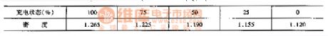
Relationship Circuit between Electrolyte Density and Charging Degree of Beijing Cherokee BJ2021
Published:2011/8/14 7:43:00 Author:Michel | Keyword: Electrolyte Density, Charging Degree, Beijing Cherokee, Relationship Circuit
First,storage battery maintenance
The storage battery needs be charged when the discharging degree is over 25%.The relationship between standard density and the charging condition is shown as table.Table:Relationship between Electrolyte Density and Charging Degree
We need to judge whehter the battery can be used by measuring the voltage of current discharging end when it does not start very well.The battery should be fully charged when it is inspected.For 58一475 battery,it needs to keep 240A discharging current and the battery is good and can be used after being charged if the voltage is not less than 9.6V.Otherwise,the battery should be replaced.The domestic 6一QA一60 battery can be used if there is no original battery. (View)
View full Circuit Diagram | Comments | Reading(795)
Charging Power Failure Alarm Circuit
Published:2011/7/23 7:39:00 Author:Michel
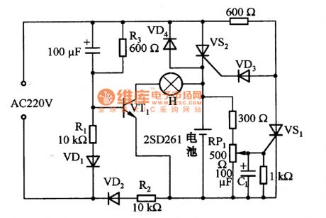
The above picture is charging power failure alarm circuit.When there is AC 220V voltage,VD1, VD2 and R1, R2 generate opposite phase,VT1 stops and H lamp does not spark.When AC is cut,battery voltage is used as power supply,VT1 is added to offset voltage via VD4 and R3.At the moment,VT1 conducts,lamp H sparks,which stands by that AC power is in power failure condition.The AC is turned on,VS2 conducts and power charges the battery.if the charging is finished,C1 is charged and provides gate triggering signal for VS1 and VS1 conducts and VS2 stops at the time.If the circuit is off,VT1 conducts lamp H sends out warning signal. (View)
View full Circuit Diagram | Comments | Reading(1690)
Infrared photoelectric type automatic faucet
Published:2011/8/24 20:58:00 Author:Christina | Keyword: Infrared, photoelectric type, automatic faucet
The Infrared photoelectric type automatic faucet is as shown in the figure.
(View)
View full Circuit Diagram | Comments | Reading(1115)
Four Independent Benchmark Voltage Source Circuit of LMl39
Published:2011/7/26 1:38:00 Author:Michel | Keyword: Benchmark, Voltage Source Circuit
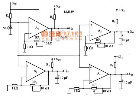

The picture is four independent benchmark voltage source circuit of LMl39.In the circuit,VD1 is used to generate benchmark voltage and comparator LM139 is the adjustable phase amplifier of four independent gains.RP1~RP4 are used to regulate the output voltage and the adjustable range is UZ≤UO≤UCC.In the formula,Uz is voltage regulating voltage of VD1 and R2~R5 are boost resistance of R2~R5 output ends.The current amplification transistor is connected to A1~A4 output ends if the output voltage is increased. (View)
View full Circuit Diagram | Comments | Reading(865)
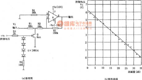
Voltage-controlled Gain Amplifier(LM307)
Published:2011/8/11 8:15:00 Author:Felicity | Keyword: Voltage-controlled, Gain Amplifier
View full Circuit Diagram | Comments | Reading(1516)
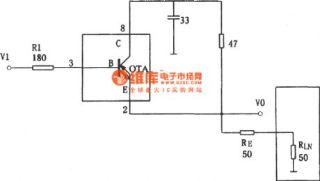
Extremely Wideband High-current Buffer
Published:2011/8/11 8:12:00 Author:Felicity | Keyword: Extremely Wideband, High-current, Buffer
View full Circuit Diagram | Comments | Reading(1044)
12MHz Broadband Buffer Composed Of OPA606
Published:2011/8/11 8:08:00 Author:Felicity | Keyword: 12MHz, Broadband Buffer
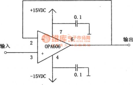
View full Circuit Diagram | Comments | Reading(788)
308 Integrated Amplifier For High Input Impedance
Published:2011/8/11 7:44:00 Author:Felicity | Keyword: Integrated Amplifier, High Input Impedance

View full Circuit Diagram | Comments | Reading(792)
High-speed Inverting Amplifier(HA5195)
Published:2011/8/11 7:55:00 Author:Felicity | Keyword: High-speed, Inverting Amplifier

View full Circuit Diagram | Comments | Reading(879)
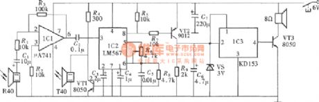
The blind source device (μA741, LM567 and KD153) (2)
Published:2011/8/13 2:16:00 Author:qqtang | Keyword: blind source device
View full Circuit Diagram | Comments | Reading(871)
The blind source device (LM567 and KD56022) (1)
Published:2011/8/13 2:24:00 Author:qqtang | Keyword: blind source device
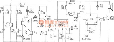
The blind always takes a stick to help them avoid obstacles when they are out of homes. As the stick can't be too long, the distance is limited. By installing a micro ultrasonic probe in the stick, not only the probing efficiency and distance can be raised, but also it's convenient to use. In the figure is the blind source device of ultrasonic probe, whose circuit is shown there. The circuit consists of the ultrasonic emitter, ultrasonic receiver and signal voltage amplifier, ultrasonic detection circuit and alarm sound circuit. (View)
View full Circuit Diagram | Comments | Reading(1923)
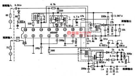
AN366,AN366P AM frequency conversion, FM AM intermediate frequency amplifier integrated circuit
Published:2011/8/25 20:11:00 Author:TaoXi | Keyword: AM, frequency conversion, FM, intermediate frequency, amplifier, integrated circuit
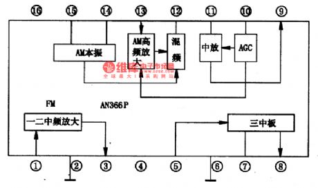
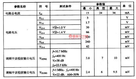
The AN366 and AN366P are designed as the AM frequency conversion, FM AM intermediate frequency amplifier integrated circuit that is produced by the Panasonic company, and this device can be used in the radio and home stereo system. The two kinds of IC have the same functions, the difference between them is the electric parameters.
1.The internal circuit block diagram and pin functions of the AN366P
The AN366P has the FM system and the AM system, the FM and AM intermediate frequency amplifier can be connected with the ceramic filter; the detection-wave output levels of the FM and AM are the same. This IC uses the dual-row DIP package, the internal circuit block diagram is as shown in figure 1-12, the pin functions and data are as shown in table 1-1.
(View)
View full Circuit Diagram | Comments | Reading(2469)
The high precision and impedance device amplifier composed of OPA2111
Published:2011/8/13 2:55:00 Author:qqtang | Keyword: high precision, device amplifier
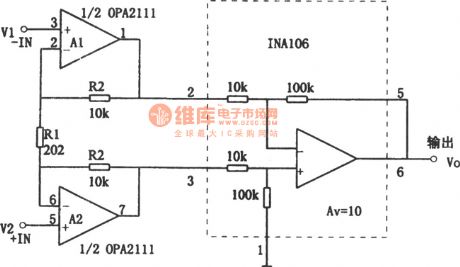
In the figure is the high precision and impedance device amplifier composed of OPA2111. The voltage of the figured circuit can be magnified to Av=10*(1+2R2/R1)=1000. The rear stage is fixed with a difference amplifier circuit whose gain is 10 times, which can expand the input common mode voltage range to ±10V. (View)
View full Circuit Diagram | Comments | Reading(830)
The equipment amplifier with the function of expanding common mode range
Published:2011/8/23 22:40:00 Author:qqtang | Keyword: equipment amplifier, common mode range
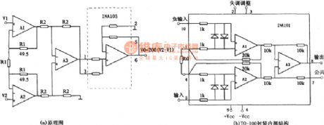
In the figure is the equipment amplifier with the function of expanding common mode range. In the circuit, A1, A2 and A4 are composed of the high-precision equipment amplifier INA10 or INA102. Seeing from the figure, the magnifying multiple of A1, A2 and A3 is 100, the rear stage amplifier is a high-precision unit gain amplifier INA105, the connection method of the amplifier is non-inverting input and follower output, i.e the 4 resistors in the circuit are in parallel connection respectively. In figure (b) is the internal structure of INA101. (View)
View full Circuit Diagram | Comments | Reading(813)
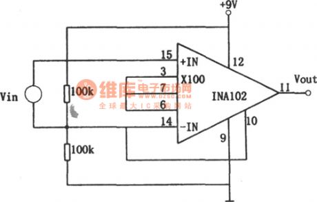
The single main power low consumption device amplifier composed of INA102
Published:2011/8/13 3:00:00 Author:qqtang | Keyword: single main power, low consumption, device amplifier
View full Circuit Diagram | Comments | Reading(739)
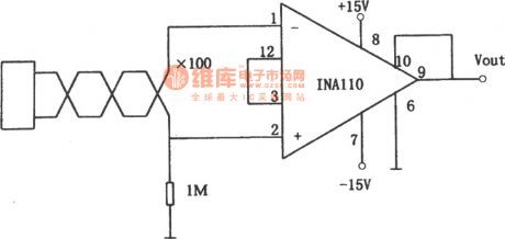
The instrument amplifier with floating signal source composed of INA110
Published:2011/8/13 3:08:00 Author:qqtang | Keyword: instrument amplifier, floating signal source
View full Circuit Diagram | Comments | Reading(834)
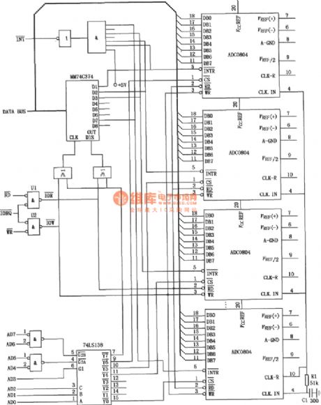
The data collecting system circuit (ADC0840)
Published:2011/8/13 2:04:00 Author:qqtang | Keyword: data collecting system
View full Circuit Diagram | Comments | Reading(797)
The micro-computer data collecting system circuit(AD7501, AD582 and AD1408)
Published:2011/8/23 22:38:00 Author:qqtang | Keyword: micro-computer, data collecting system
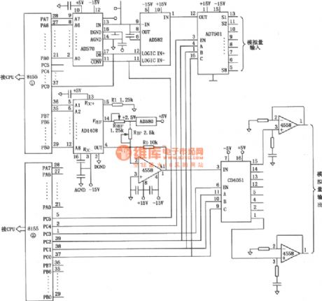
The micro-computer data collecting system circuit composed of AD570, AD1408 and micro-processor CPU8155 is shown in the figure. The circuit under test has 8 channels, each channel is tested in sequence, the scanning of each channel is not more than 50μs, the system logic LEV is TTL, binary system code, the data transmission is parallel.
(View)
View full Circuit Diagram | Comments | Reading(1052)
| Pages:60/250 At 204142434445464748495051525354555657585960Under 20 |
Circuit Categories
power supply circuit
Amplifier Circuit
Basic Circuit
LED and Light Circuit
Sensor Circuit
Signal Processing
Electrical Equipment Circuit
Control Circuit
Remote Control Circuit
A/D-D/A Converter Circuit
Audio Circuit
Measuring and Test Circuit
Communication Circuit
Computer-Related Circuit
555 Circuit
Automotive Circuit
Repairing Circuit