
Amplifier Circuit
Index 49
Common-mode voltage reaches + 1000V Differential amplifier circuit with INA110
Published:2011/8/30 2:48:00 Author:Jessie | Keyword: Common-mode voltage, Differential amplifier
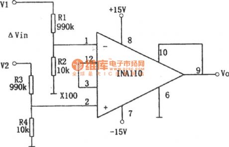
As shown in figure, the circuitis common-mode differential amplifying circuit with the input voltagebeing+ 1000V. This circuit adopts mosfet (FET) input apparatus using amplifierINA110 and input resistance bleeder. Reverse phase input and in-phase input is respectivelycomposedof R1, R2 and R3, R4.Because R1=R3, R2=R4, the attenuation ratio of voltage divider is: K=R2/(R1+R2)=10/(10+990)=1/100. (View)
View full Circuit Diagram | Comments | Reading(1406)
Driver 50 Ω load linear amplifier circuit
Published:2011/8/30 2:45:00 Author:Jessie | Keyword: Driver 50 Ω load, linear amplifier
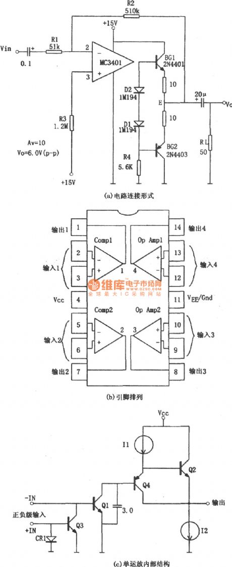
As shown in the chart, the circuitis the driver 50 Ω load linear amplifier circuit. This circuit consists of two components. The former stage is composedof thechip MC3401 and affiliated circuit, and the laststage is the OTL complementary symmetry power amplifier circuit. R2 is introduced tovoltage parallel negative feedback to improve the dynamic index. (View)
View full Circuit Diagram | Comments | Reading(957)
Low distortion AGC amplifier (AD824) diagram
Published:2011/8/30 2:31:00 Author:Jessie | Keyword: Low distortion, AGC amplifier
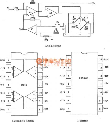
In communications, control and remote sensing system, the low distortion automatic gain control circuit is needed. As shown in diagram, the circuit is the low-distortion AGC amplifier. A1 is the amplifier. A2 is the voltage following device, which is used asisolation level to introduce feedback for amplifier A1. Integrated amp in (A) can be proper selected according to actual needs. If you hope the single power supply, you can choose low powerfour operational amplifiercircuit AD824A or AD824B; If you hope to adopt double power supply, you can use μPC4074 four operational amplifier integrated chip. (View)
View full Circuit Diagram | Comments | Reading(1780)
6z4 Tube amp circuit
Published:2011/8/29 20:56:00 Author:Jessie | Keyword: Tube amp
Voltage amplifier tube canreplace 6N1, thenR4 reduces to100kΩ, R10 reduces to50kΩ. 6Z4 can replace power rectifier electronic diode. Because single 6Z4'smaximumDC output current is only 75mA,it should use two tubes connected in parallel. It also can use semiconductor diode to replace it. (View)
View full Circuit Diagram | Comments | Reading(5680)
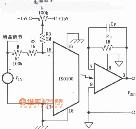
Unipolarity isolation test instrumentation amplification circuit composed of ISO100 with detuning adjustment
Published:2011/8/30 1:36:00 Author:Jessie | Keyword: Unipolarity isolation , test instrumentation amplification, detuning adjustment
View full Circuit Diagram | Comments | Reading(773)
The detector amplifier without cooling
Published:2011/11/30 21:35:00 Author:May | Keyword: detector amplifier, without cooling
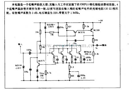
This circuit is a low-noise amplifier, its input isconnected with ORP10 lndium antimonide detector workingunder room temperature . Four low noise transistors are connected inparallelfor thefirst step in order to match with low noise level photoresistor (30Ω) connected in input end. Effective noise figure is 3dB, voltage gain is 220, bandwidth is above 1MHz.
(View)
View full Circuit Diagram | Comments | Reading(858)
Low noise 8GHz small signal amplifier circuit diagram
Published:2011/11/3 0:47:00 Author:May | Keyword: small signal amplifier, Low noise small signal amplifier, 8GHz small signal amplifier
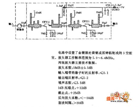
Low noise 8GHz small signal amplifier circuit diagram is shown in the following diagram:
In the circuit, it sets three cavity chambersmade of silvering brass or aluminum. The working frequency range of amplifier is 5.9~6.4MHz.Main technology data of two level amplifer:amplification factor: 18dB±0.5dBReflectivity when input end carrys insulator: ≤0.1output end reflectivity: ≤0.2noise factor:≤3.5dB1dB compression point: +12dBcut off point: +25dBreverse amplification factor: <-50dBharmonic interval: >30dB (View)
View full Circuit Diagram | Comments | Reading(1149)
1000MHz two-level broadband amplifier circuit diagram
Published:2011/10/31 3:54:00 Author:May | Keyword: 1000MHz , two-level broadband amplifier
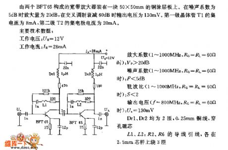
Wide-band amplifier composed of two BFT65 is packaged in one 50×50mm copper coated board. When noise factor is 0.5dB, the gain is 20dB; when crossover modulation attenuation is60dB, theoutput voltage is 130mV. The first level transistor T1 intergrated current is 8mA, the second level T2 collector current is 20mA.
Main technical data:
work voltage: UB=12Vwork current: Ib=28mAamplification factor ( when 1~1000MHz, RC=RL=60Ω) : VP>20dBnoise factor ( when 1~1000MHz, RC=RL=60Ω) : F<5dBstanding-wave ratio ( when 1~1000MHz, RC=RL=60Ω) : S<2output voltage ( when f=800MHz, RC=RL=60Ω) : Ua=130mV (View)
View full Circuit Diagram | Comments | Reading(1410)
Cheap solid amplifier circuit diagram
Published:2011/10/27 21:41:00 Author:May | Keyword: solid amplifier
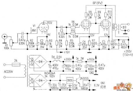
μ voltage amplifying tube 6N1 (1/2) is made in the single-stage self-sufficient bias voltage amplifier with the gain K=20, when it is input 0.6V active voltage, it outputs 12V signal voltage to make the backward stage reach the specified output power 11W, which can definitely satisfy with each kind of sound source connection. The backward stage of power amplifier uses two 6P13P connected in parallel, which is used as the single-end Class A power output, and the loaded impedance is 1300Ω. Because the complete machine's distortion is not very high, therefore it will omit the negative feedback ring circuit to exhibit broad sound field. The 6P13P filament is supplied by AC 6.3V, and the 6N1 filament is supplied by the DC power supply. (View)
View full Circuit Diagram | Comments | Reading(2398)
Medium power linear amplifier pin circuit
Published:2011/11/2 21:02:00 Author:May | Keyword: power linear amplifier
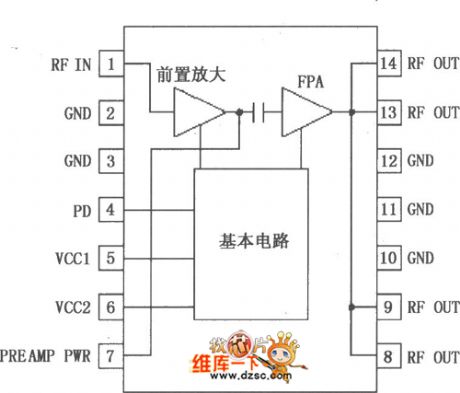
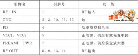
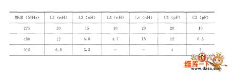
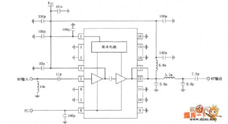
RF2103P is thepower linear amplifier IC, which uses advanced GaAs heterojunction bipolar transistor (HBT), and it is designed for UHF frequency wireless transmit final linear RF amplifier, and its working frequency is 450~1000MHz. RF2103P also can be used as driver amplifier to applyin higher power situation, and the device includes power supply wire, bypass capacitor and matchingnetwork, and itcan generate 750mW (CW) output power. RF2103 can besupplied by 3 batteries, and the maximum CW is 175mW when output is 3.6V, and the device's total gain is 31dB. RF2103P can be used for digital communication system, spread spectrum communication system as high power linear driver. RF2103P pin array is shown in the picture.
Pin function is shown in the following diagram:
(View)
View full Circuit Diagram | Comments | Reading(726)
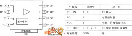
RF amplifier principle circuit composed of RF2103P
Published:2011/10/26 21:11:00 Author:May | Keyword: RF amplifier
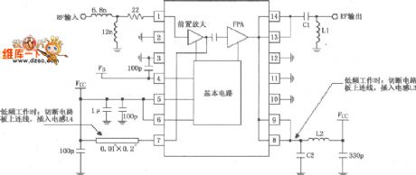
RF signal (RF) isinput by pin 1, enlarged by preamplifier and final power amplifier ( FPA), thenoutput by pin 14. There is a blocking coupling capacitor between pin 1 and preamplifier, so it does not need to add coupling capacitor. Output ends pin 8, 9, 13, 14 are connected inside of the chip. Normally, pin 13, 14 are connected outside to be uses the as signal output, which connects to the matching network to make the amplifier output resistance match with it, then it gets themaximum output power and efficiency; and pin 8, 9 are connectedoutsideto beas power supply end, when it works at 915MHz, it adds a filter capacitor C2(=2pF) to ground tomake up filter circuitwith second harmonic, which can shortconnect second harmonic effectively.
(View)
View full Circuit Diagram | Comments | Reading(1321)
Medium power amplifier RF2104 pin circuit
Published:2011/10/26 21:27:00 Author:May | Keyword: Medium power amplifier
RF2104 is the medium power amplifier IC, and the design is used in UHF frequency band radio transmitting last stage linear RF enlarging, and the operating frequency is 400~1000MHz. RF2104 can be used as the driver amplifier to apply in the high power situation, and it uses the square bat-flyaway 16-lead seal. RF2104 can be supplied by 3-battery power supply, and the biggest CW output is +27dBm when the power is 3.6V, the component overall gain is 26dB. RF2104 is used in 900MHz ISM frequency band, 400MHz industry radio traffic, high-power driver, portable battery supply set, commercial and the consumer system, base depot equipment and so on. (View)
View full Circuit Diagram | Comments | Reading(900)
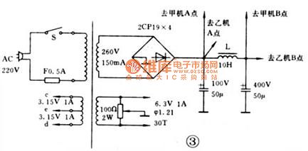
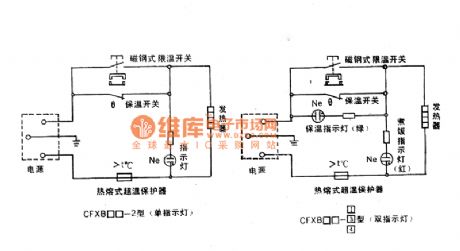
Rongsheng heat insulation automatic electric cooker principle diagram
Published:2011/8/30 1:40:00 Author:Jessie | Keyword: Rongsheng , heat insulation, automatic electric cooker
View full Circuit Diagram | Comments | Reading(836)
830MHz medium power amplifier principle circuit composed of RF2104
Published:2011/10/26 21:36:00 Author:May | Keyword: medium power amplifier principle
Radio-frequency signal (RF) is input by pin 5, output by pin 12 after being amplified by the pre-amplifier, last stage power amplifier. pin 5 has the DC voltage, therefore it is added the separating direct coupling capacitor and simultaneously connected to divergence inductance (10nH) in parallel, pin 5's input impedance is 50Ω. The output end's pin 12, 13 are connected, usually, pin 13, 14 are connected outside to be used as the signal output, and the output connects the matching network to make the amplifier output impedance match with it, when the pin's loaded impedance is 5+10Ω, itmay obtain the peak power output. pin 13, 14 are connected outside to be used as the last stage power amplifier's power source end. (View)
View full Circuit Diagram | Comments | Reading(785)
RF2126 high power linear amplifier pin circuit diagram
Published:2011/10/26 22:00:00 Author:May | Keyword: high power linear amplifier
RF2126 is high-power, high-efficiency linear amplifier IC. It adopts advanced GaAs hetero-junction bipolar transistor (HBT) technology. It is designed for 2.5GHz ISM frequency range final linear RF amplifier, such as WLAN and POS terminal, it also can beused for digital PCS phone to send out final linear enlarging. Its working frequency is 1800~2500MHz.RF2126 has matching network, and RF2126 itself includes power supply wire and bypass capacitor. Output power’s typical value is 1W. RF2126 can beused for 2.5Hz ISM frequency range, digital communication system, PCS communications system, commercial and consumer system, portable battery power equipment and so on. RF2126’s pin array and functionare shown in the following diagram.
(View)
View full Circuit Diagram | Comments | Reading(1039)
Operation amplifiering instrumentation amplifier circuit
Published:2011/8/24 2:13:00 Author:Jessie | Keyword: Operation amplifiering, instrumentation amplifier
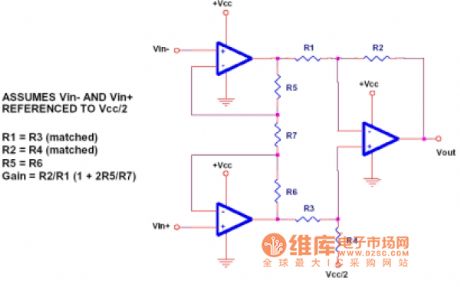
Instrumentation amplifier is usedin the occasion whereneed to amplifier small level signalDC signal, andit is produced by minus skulls topology. Instrument amplifierhas the advantage of in-phase input's high impedance. This circuit is the basic instrument amplifier circuit, other instrumentation amplifiers areshown in the figure, here the input also use a single power supply. This circuit is actually a single power strain gauge. This circuit's fault is need completely equal resistance, otherwise this circuit's common mode rejection ratio will be very low. (View)
View full Circuit Diagram | Comments | Reading(1260)
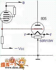
805 single end power amplifier circuit
Published:2011/10/26 22:11:00 Author:May | Keyword: single end, power amplifier
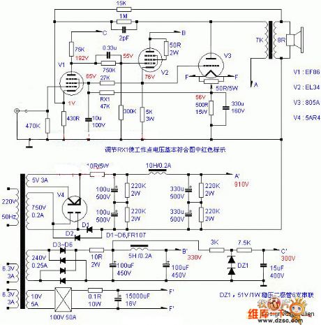
It isthe 805 single end circuit with proper performance. Its debugging is very simple. Push level upraises 805’s cathode potential even though itdoes not add negative voltage supply. And this is equivalent to add push range. The whole adds some loop feedback and it can not cause thetone impaired problem. It needs to take notethat the supply voltage of 805’s filament should bein the range of 10V ±0.2V and the output power is higher than 25W. (View)
View full Circuit Diagram | Comments | Reading(3539)
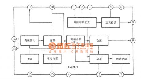
Samsung KA22471 FM AM intermediate frequency amplifier circuit diagram
Published:2011/8/19 2:24:00 Author:Jessie | Keyword: Samsung, FM AM , intermediate frequency amplifier
View full Circuit Diagram | Comments | Reading(1994)
Operation amplifier subtracter circuit diagram
Published:2011/8/19 2:23:00 Author:Jessie | Keyword: Operation amplifier subtracter
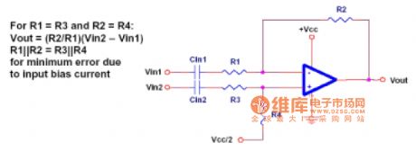
Like adder, figure8 is a subtracter. It is used to remove the original singer's voices in stereo cassettes and leave the accompaniment ( When recording, the two channels' originalvoice's levelis the same, but the accompaniment's is not). (View)
View full Circuit Diagram | Comments | Reading(701)
805 Vacuum tube transformer push power amplifier circuit
Published:2011/5/13 4:49:00 Author:May | Keyword: power amplifier, Vacuum tube, transformer push
The 805’s features of high essential resistance leads to that the inductance value output transformer needed is larger. In addition, the other problem caused by it is that output impedance is too high and damping coefficient is decreased. It is a common 805 circuit without transformer secondary sampling negative feedback. Its damping coefficient is 10K/tube essential resistance (10K)=1 and is lower when output transformer’s primary impedance is 10K. And it is lacking proper controlling force to speaker. Low frequency has lager quantity but low quality.
Also, the damping coefficient of 300B vacuum tube with 700Ω essential resistance is 3.5K/700Ω=5 and it has effective controlling force to speaker when it adopts 3.5K output transformer. So, the 805 class essential resistance tube should add negative feedback which the sampling point is output transformer’s primary, and the familiar is negative feedback loop. It can make the essential resistance of 805 decreasing some by suitable decreasing the working voltage (suitable decrease output power) and improving 805 working current (with litter influence the designing and making of output transformer). But it is not the main method. (View)
View full Circuit Diagram | Comments | Reading(2608)
| Pages:49/250 At 204142434445464748495051525354555657585960Under 20 |
Circuit Categories
power supply circuit
Amplifier Circuit
Basic Circuit
LED and Light Circuit
Sensor Circuit
Signal Processing
Electrical Equipment Circuit
Control Circuit
Remote Control Circuit
A/D-D/A Converter Circuit
Audio Circuit
Measuring and Test Circuit
Communication Circuit
Computer-Related Circuit
555 Circuit
Automotive Circuit
Repairing Circuit