
Amplifier Circuit
Index 43
LM3860,325W Audio Amplifier
Published:2012/10/12 22:11:00 Author:muriel | Keyword: LM3860,325W, Audio Amplifier
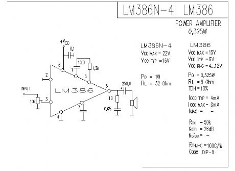
The LM386 is a power amplifier designed for use in low voltage consumer applications. The gain is internally set to 20 to keep external part count low, but the addition of an external resistor and capacitor between pins 1 and 8 will increase the gain to any value from 20 to 200.
The inputs are ground referenced while the output automatically biases to one-half the supply voltage. The quiescent power drain is only 24 milliwatts when operating from a 6 volt supply, making the LM386 ideal for battery operation.
(View)
View full Circuit Diagram | Comments | Reading(1878)
Improved 3 Transistor Audio Amp (80 milliwatt)
Published:2012/10/11 21:32:00 Author:muriel | Keyword: Improved, 3 Transistor, Audio Amp, 80 milliwatt
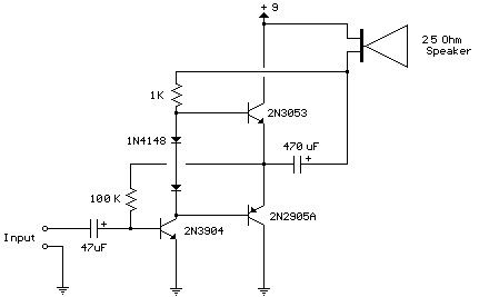
This circuit is similar to the one above but uses positive feedback to get a little more amplitude to the speaker. I copied it from a small 5 transistor radio that uses a 25 ohm speaker. In the circuit above, the load resistor for the driver transistor is tied directly to the + supply. This has a disadvantage in that as the output moves positive, the drop across the 470 ohm resistor decreases which reduces the base current to the top NPN transistor. Thus the output cannot move all the way to the + supply because there wouldn't be any voltage across the 470 resistor and no base current to the NPN transistor.
This circuit corrects the problem somewhat and allows a larger voltage swing and probably more output power, but I don't know how much without doing a lot of testing. The output still won't move more than a couple volts using small transistors since the peak current won't be more than 100mA or so into a 25 ohm load. But it's an improvement over the other circuit above.
In this circuit, the 1K load resistor is tied to the speaker so that as the output moves negative, the voltage on the 1K resistor is reduced, which aids in turning off the top NPN transistor. When the output moves positive, the charge on the 470uF capacitor aids in turning on the top NPN transistor.
(View)
View full Circuit Diagram | Comments | Reading(1080)
3 Transistor Audio Amp (50 milliwatt)
Published:2012/10/11 21:31:00 Author:muriel | Keyword: 3 Transistor, Audio Amp, 50 milliwatt
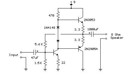
Here is a little audio amplifier similar to what you might find in a small transistor radio. The input stage is biased so that the supply voltage is divided equally across the two complimentary output transistors which are slightly biased in conduction by the diodes between the bases. A 3.3 ohm resistor is used in series with the emitters of the output transistors to stabilize the bias current so it doesn't change much with temperature or with different transistors and diodes. As the bias current increases, the voltage between the emitter and base decreases, thus reducing the conduction. Input impedance is about 500 ohms and voltage gain is about 5 with an 8 ohm speaker attached. The voltage swing on the speaker is about 2 volts without distorting and power output is in the 50 milliwatt range. A higher supply voltage and the addition of heat sinks to the output transistors would provide more power. Circuit draws about 30 milliamps from a 9 volt supply.
(View)
View full Circuit Diagram | Comments | Reading(1705)
TDA 2030 8W Audio Amplifier
Published:2012/10/11 21:19:00 Author:muriel | Keyword: TDA 2030, 8W, Audio Amplifier
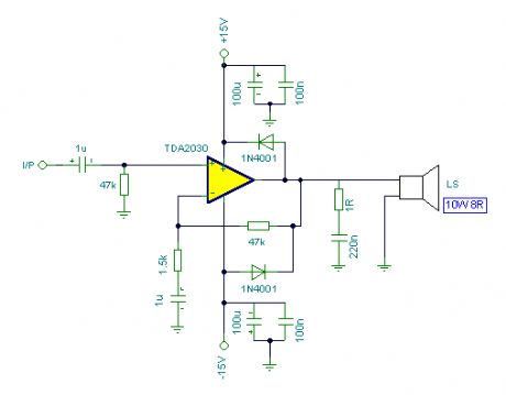
TDA 2030 audio amplifier can output 20 W but in this schematic we have reduced the power to 8w and we use 10w speakers. The input sensivity is around 200mV and the amplifier is set by the 47k and 1.5k resistors.
TDA2030 amplifier circuit diagram
(View)
View full Circuit Diagram | Comments | Reading(2013)
TDA1514 50W Hi Fi audio amplifier
Published:2012/10/11 21:18:00 Author:muriel | Keyword: TDA1514, 50W, Hi Fi, audio amplifier
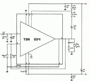
TDA1514 is a hi fi audio amplifier which can output 50W audio power. The power supply is between 10V and 30V. It can be used as a home amplifier.The TDA1514 integrated circuit is a hi-fi power amplifier for use as a building block in radio, tv and other audio applications. The TDA 1514 circuit is totally protected, also has a mute function that can be arranged for a period after power-on with a delay time fixed by external components. The device is intended for symmetrical power supplies but an asymmetrical supply may also be used. For stereo amplifier configuration use two identical circuits.
TDA1514 amplifier
(View)
View full Circuit Diagram | Comments | Reading(1736)
Stereo car audio amplifier TDA1557Q TDA1553Q
Published:2012/10/11 21:18:00 Author:muriel | Keyword: Stereo car, audio amplifier, TDA1557Q, TDA1553Q
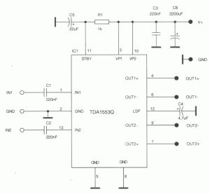
This stereo amplifier is for car purpouse and can deliver up to 2 x 22W using a single TDA1557Q or TDA1553Q from Philips.TDA1557Q TDA1553Q datasheet (View)
View full Circuit Diagram | Comments | Reading(2412)
STK4241V Home Stereo Amplifier
Published:2012/10/11 21:17:00 Author:muriel | Keyword: STK4241V, Home, Stereo Amplifier
This Home Stereo Amp is equiped with STK4241V wich is a thick film hybrid IC, AF Power Amplifier (Split Power Supply) (120W+120W min, THD = 0.08%). STK4241V has some features like:? Muting circuit built-in to isolate all types of shock noise? Current mirror circuit for low 0.08% total harmonic distortionFor this 2x120W home stereo power audio amplifier we use a single monochip STK4241V to obtain up to 120W for each channel.
STK4241V amplifier circuit diagram
(View)
View full Circuit Diagram | Comments | Reading(1657)
Audio power amplifier 50W 2N3055 MJ2955
Published:2012/10/11 21:16:00 Author:muriel | Keyword: Audio, power amplifier, 50W, 2N3055, MJ2955
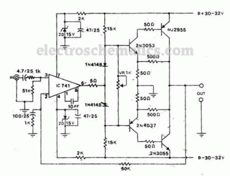
A very simple audio power amplifier circuit built with 741, 2N3053, 2N4037, 2N3055 and MJ2955 which deliver up to 50W on a 8Ω speaker.Use a 3A symmetric power supply for mono application and a 5A for stereo power amplifiers. Please take good precaution when use this audio amplifier : do not shortcircuit the output or not connect speakers ! Always check twice !
2N3055 audio amplifier circuit schematic
(View)
View full Circuit Diagram | Comments | Reading(3676)
Wideband VHF preamplifier
Published:2012/10/11 21:11:00 Author:muriel | Keyword: Wideband, VHF, preamplifier
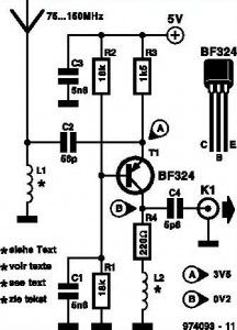
This inexpensive VHF preamplifier uses the BF324 TO92 style pnp transistor in a grounded-base configuration. The circuit may be used as a signal booster with VHF receivers whose front end suffers from low sensitivity (such as many valved and army surplus types). The frequency range of the preamplifier is roughly from 75MHz to 150MHz. The two inductors in the circuit are home made. L1 consists of 10turns of 24SWG enamelled copper wire; the internal diameter is 3mm, no core. Inductor L2 has 13 turns of the same wire, and an internal diameter of 5mm; no core is used either. A construction tip: close-wind the inductors using 3 and 5mm drill bits respectively as temporary formers.
The prototype of the preamplifier was successfully used with an 88-108 MHz FM broadcast receiver and a 2-metre VHF ham receiver. The preamplifier draws about 2.5mA from a 5-volt supply.
Wideband VHF preamplifier circuit schematic
(View)
View full Circuit Diagram | Comments | Reading(3190)
Single-Chip VHF RF Preamplifier
Published:2012/10/11 21:10:00 Author:muriel | Keyword: Single-Chip, VHF, RF, Preamplifier
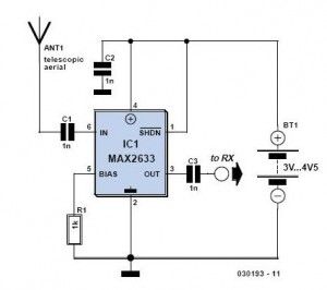
Here is a high performance RF amplifier for the entire VHF broadcast and PMR band (100-175 MHz) which can be successfully built without any special test equipment. The grounded-gate configuration is inherently stable without any neutralization if appropriate PCB layout techniques are employed. The performance of the amplifier is quite good.
The noise figure is below 2 dB and the gain is over 13 dB. The low noise figure and good gain will help car radios or home stereo receivers pick up the lower-power local or campus radio stations, or distant amateur VHF stations in the 2-metres band. Due to the so-called threshold effect, FM receivers loose signals abruptly so if your favourite station fades in and out as you drive, this amplifier can cause a dramatic improvement.
The MAX2633 is a low-voltage, low-noise amplifier for use from VHF to SHF frequencies. Operating from a single +2.7 V to +5.5V supply, it has a virtually flat gain response to 900 MHz. Its low noise figure and low supply current makes it ideal for RF receive, buffer and transmit applications. The MAX2633 is biased internally and has a user-selectable supply current, which can be adjusted by adding a single external resistor (here, R1). This circuit draws only 3 mA current.
VHF RF preamplifier circuit diagram
Besides a single bias resistor, the only external components needed for the MAX2630 family of RF amplifiers are input and output blocking capacitors, C1 and C3, and a VCC bypass capacitor, C2. The coupling capacitors must be large enough to contribute negligible reactance in a 50-Ω system at the lowest operating frequency. Use the following equation to calculate their minimum value:Cc = 53000/ flow [pF]
(View)
View full Circuit Diagram | Comments | Reading(1316)
Low voltage microphone preamplifier
Published:2012/10/11 21:09:00 Author:muriel | Keyword: Low voltage, microphone preamplifier
This is a low voltage microphone preamplifier circuit with a 1.5V power supply. The reference, with a 500 kHz unity-gain bandwidth, is used as a preamplifier with a gain of 100. Its output is fed through a gain-control potentiometer to the op amp, which is connected for a gain of 10. The combination gives a 60 dB gain with a 10 kHz bandwidth, unloaded, and 5 kHz loaded at 500 Ω . Input impedance is 10 kΩ.Potentially, using the reference as a preamplifier in this fashion can cause excess noise. However, because the reference voltage is low, the nose contribution, which adds root-mean-square, is likewise low. The input noise voltage in this connection is 440-500 nV Hz, about equal to that of the amp.
Microphone preamplifier circuit diagram
(View)
View full Circuit Diagram | Comments | Reading(1175)
70MHz RF power amplifier
Published:2012/10/11 21:08:00 Author:muriel | Keyword: 70MHz, RF, power amplifier
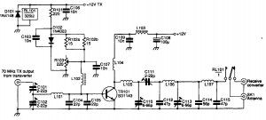
This 70MHz rf power amplifier circuit uses the SD1143 transistor which provides a gain of about 14dB in this design. It uses the fact that a 175MHz device has a much higher gain when used at lower frequencies. The amplifier was originally designed to be used with a transverter. The output is 8 to 10W for a 300 to 500 mW input power. Unfortunately, we dont have the coils values. With a few modifications you can use this amplifier for different frequencies.
70MHz power amplifier circuit diagram
(View)
View full Circuit Diagram | Comments | Reading(1460)
BLW96 amplifier
Published:2012/10/11 2:26:00 Author:muriel | Keyword: BLW96,amplifier
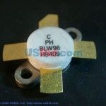
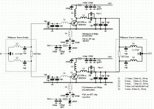
BLW96 is a HF/VHF power transistor intended for use in class-A, AB and B operated high power industrial and military transmitting equipment in the h.f. and v.h.f. band.
BLW96 amplifier 450W 50MHz
A possible downside of this is that they may not have less gain at 50MHz compared to a VHF transistor but, as can be seen in Figure 1, at least 12 to 14dB of gain can be obtained at 50MHzz (the BLW96 performs well at 70MHz as well incidentally).To achieve the required output in this design, two BLW96s have been paralleled to provide 450 watts with just a little over 20 watts of drive. The input power is split using a Wilkinson power divider whose design was extensively discussed in SIX NEWS #33, The output of the two amplifiers are combined using the same, only reversed, circuit. Under normal circumstances the 100 ohm resistor connecting the two output (or input) ports does not dissipate very much power, but during tune-up it is possible that it could.
As it is important that these resistors are truly non-inductive, the design uses rather special devices.These are ‘bolt-down’ 100 Ohm terminating resistors with two flying leads to connect to the circuit board – they look rather like transistors in construction. (View)
View full Circuit Diagram | Comments | Reading(1637)
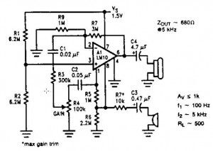
HiFi Headphone Amplifier circuit
Published:2012/10/10 1:56:00 Author:muriel | Keyword: HiFi Headphone, Amplifier
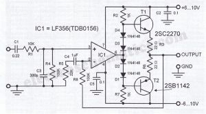
This HiFi headphone amplifier circuit design is normally used to drive a headphone with a relative low impedance. It provides one watt power output and it can also be applied as an output stage for preamplifiers in conjuction with active loudspeakers boxes. The headphone amp is composed of an OP-AMP and an additional transistor amplifier. Input signals pass through a low pass filter composed of R1-C2. Its applification together with a relatively “fast” OPAMP provides a low distortion factor.The standby current is preset by diodes D1…D4 and R7-R8. The feedback resistors R3 and R4 set the amplification factor at about 15 dB. The distorsion factor is aound 0.1 % with a bandwidth of 10 Hz to 30 kHz.The headphone amplifier provides a maximum output of 1 watt to an 8 ohm load by an input level of 500 mV. High impedance headphones can be connected. The circuit can also drive a 4 ohm speaker.
Headphone amp circuit diagram
In order to prevent the output transistors from being destroyed in case of an output short circuit, they must be heatsinked. The transistors must also be electrically isolated from heatsink. Supply voltage can be provided by an adaptor with 6-8 volts DC output.
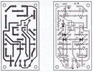
Headphones amplifier PCB layout
(View)
View full Circuit Diagram | Comments | Reading(2535)
Car Antenna Amplifier circuit
Published:2012/10/10 1:55:00 Author:muriel | Keyword: Car Antenna, Amplifier
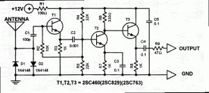
This car antenna amplifier can be used up to 70 MHz and is specially designed to boost the weak signals captured by the car antenna.It has a high input impedance and a low noise figure.
The total gain of the car antenna amplifier is around 30 dB and the input impedance at 30 Mhz is around 10 KΩ. The amplifier must be mounted directly at the base of the antenna to avoid signal losses caused by the capacitive character of the coaxial cable.This antenna amp must be used for non-mobile recievers. If you intend to install this circuit in you outdoor mounted antenna, make sure that is housed in a water proof case. Use this car antenna amp circuit only for receiver antennas. Transmitting through it will damage the components.
Car Antenna Amp Circuit Diagram
Antenna Amplifier PCB Layout
(View)
View full Circuit Diagram | Comments | Reading(1486)
Electret microphone amplifier circuit
Published:2012/10/10 1:53:00 Author:muriel | Keyword: Electret microphone, amplifier
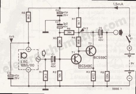
This article describes an compact electret microphone amplifier but you can connect dynamic microphones with low resistance. Electret microphones can be inserted in the same box with the amplifier, it only need 5 to 10V or 9V battery with a current consumption of just 1.5mA.
Electret microphone amplifier circuit
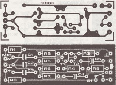
Electret mic amplifier pcb
(View)
View full Circuit Diagram | Comments | Reading(2864)
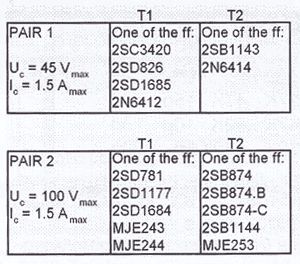
Rf 15W – 30W power amplifier KT922, KT930, KT934
Published:2012/10/10 1:53:00 Author:muriel | Keyword: Rf, 15W – 30W, power amplifier
This rf amplifier ensure the power you need to boost a small transmitter.Depending of input rf power, power supply and transistor, this amplifier can boost from 15W up to 30W.The most important components : 7805, 1N4001 diodes mounted in series, 120 ohm / 2W resistor and 1N4145 diodes.The setup : trim P (220 ohm ) untill you obtain 50mA thru T1 and 100mA thru T2. Without any input signal you must measure 1.5V like in the schematic, if the voltage is higher the 2 transistors can burn.At 12V and 0.1W input rf power the output is 6W and with 0.5W the output is 15W.At 24V and 0.1W input power the output is 10W and with 0.5W the output is 25W.
RF power amplifier circuit diagram
(View)
View full Circuit Diagram | Comments | Reading(2183)
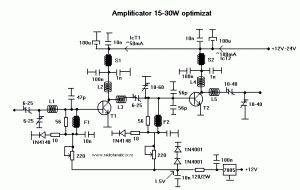
25W FM radio amplifier circuit
Published:2012/10/10 1:51:00 Author:muriel | Keyword: 25W, FM, radio amplifier
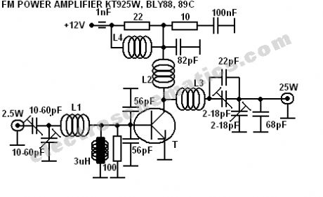
A simple 25W fm radio amplifier used as a final stage for a 2.5W transmitter. I has a total gain of 10 dB and needs a 12V / 3A power supply. It is equiped with KT925W or BLY88, BLY89C. Use a very good headsink because this transistor get very hot Coils values:L1 = L3 = 4 turns / 1.5mm / 8mm / 10mm longL2 = 4 turns / 1mm/6mm/10mm longL4 = 20 turns / 0.8mm / on 22Ω resistor
25W FM radio amplifier circuit schematic
(View)
View full Circuit Diagram | Comments | Reading(1604)
The circuit of high-fidelity amplifier
Published:2012/10/9 22:30:00 Author:Ecco | Keyword: high-fidelity amplifier
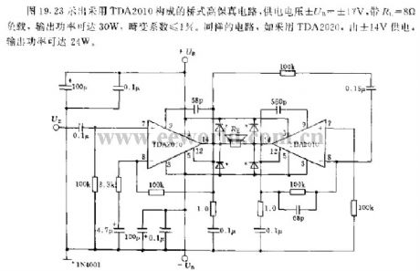
Figure 19.23 shows bridge high-fidelity circuit with TDA2010, and the supply voltage ± UB = ± 17V, load RL = 8Ω, output power can be up to 30W, the distortion coefficient ≤ 1 % . If the same circuit uses TDA2020, ± 14V power supply, the output power can be up to 24W.
(View)
View full Circuit Diagram | Comments | Reading(1536)
The circuit of measuring bridge amplifier
Published:2012/10/9 22:25:00 Author:Ecco | Keyword: Measuring bridge , amplifier

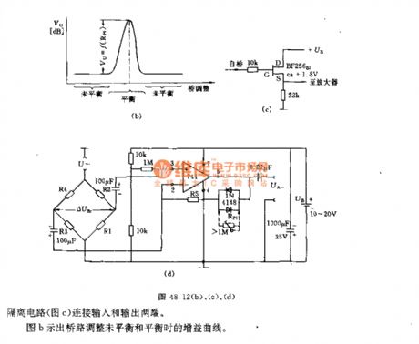
The measurement circuit shown in figure a is composed of resistors R1 ~ R4, the output voltage UBr may be DC or AC voltage ( up to 100kHz), if it is AC voltage, it can use capacitive coupling (Figure d ). In both cases, it can use high ohmic isolation circuit (Figure c) to connect to the input and output ends. Figure b shows unbalanced and balanced adjustment gain curve of bridge circuit.
(View)
View full Circuit Diagram | Comments | Reading(1217)
| Pages:43/250 At 204142434445464748495051525354555657585960Under 20 |
Circuit Categories
power supply circuit
Amplifier Circuit
Basic Circuit
LED and Light Circuit
Sensor Circuit
Signal Processing
Electrical Equipment Circuit
Control Circuit
Remote Control Circuit
A/D-D/A Converter Circuit
Audio Circuit
Measuring and Test Circuit
Communication Circuit
Computer-Related Circuit
555 Circuit
Automotive Circuit
Repairing Circuit