
Amplifier Circuit
Index 56
2A3A tube push-pull power amplifier circuit
Published:2011/9/25 22:26:00 Author:Ecco | Keyword: tube , push-pull , power amplifier
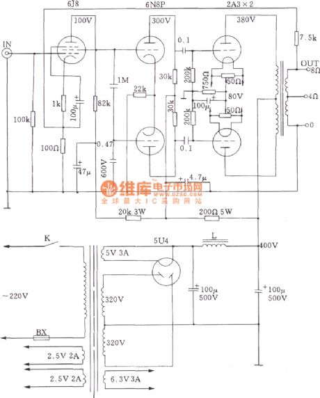
2A3 is a low ESR and direct-thermal transistor, and the internal resistance is only 800Ω, so the output transformer primary screen load impedance needs 3.5kΩ. Push-pull power amplifier tube's screen voltage takes 360 ~ 380V, cathode-to-ground voltage is 60 ~ 80V, and the total operating current of amplifier is 80 ~ 100mA, the maximum output power is up to 15W. Local distortion factor is 1% to 2%, and frequency response is ± 2dB in the range of 20Hz ~ 40kHz. (View)
View full Circuit Diagram | Comments | Reading(2921)
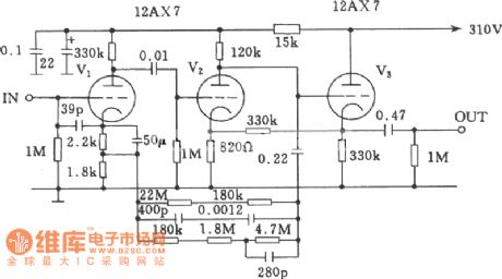
McIntosh-C22 tube preamp equalizer amplifier circuit diagram
Published:2011/9/25 21:57:00 Author:Ecco | Keyword: tube , preamp equalizer amplifier
View full Circuit Diagram | Comments | Reading(5168)
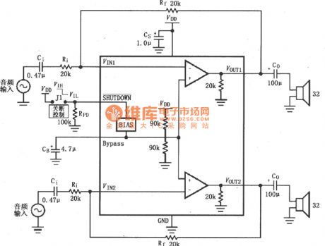
The typical circuit diagram of LM4916 for binaural amplifier
Published:2011/8/22 22:18:00 Author:Rebekka | Keyword: Two-channel amplifier
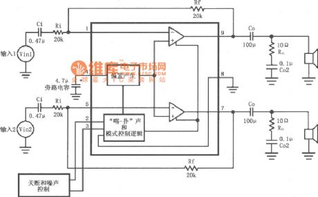
Pin 1 and 5 of LM4916 are inputed seperately by left and right channel audio signals and outputed respectively by pin 9, 7 after being amplified by the internal amplifier. Through Coupling capacitor Co adding to since channel speaker. The pin 2 of LM4916 connects shutdown control. It is allowed to work when pin 2 connects with VDD; It is not allowed to when it connetcs to a low level or it will decrease chip power consumption. The pin3 of LM4916 is squelch control. It is squelch mode when pin 3 connects to a low level. In order to eliminate the Cameroon - flapping sound that caused by switching transitions. It is allowed to work when it connects to a high level. (View)
View full Circuit Diagram | Comments | Reading(1168)
LM4911 typical application circuit diagram for dual-channel amplifier
Published:2011/8/22 22:16:00 Author:Rebekka | Keyword: MSOP, dual-channel amplifier
Left and right channel audio signals areinputto 1,5 feet of LM4911 (MSOP packaging)respectively. They are output by 9, 7, 8 feet after being amplified by the internal amplifier. They will be added to the respective channel speaker through coupling capacitor. Maximum power of the amplifier is PDMAX = VDD2/2π2RL (output capacitive coupling mode). LM4911's 2 feetis connected shutdown Control outside. It is allowed to work when 2 feet connected VDD (high level). It is not allowed to work when then low (ground) because it will reduce chip power consumption. (View)
View full Circuit Diagram | Comments | Reading(892)
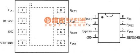
LM4910 stereo headphone amplifier circuit diagram
Published:2011/8/31 2:32:00 Author:Rebekka | Keyword: stereo headphone amplifier
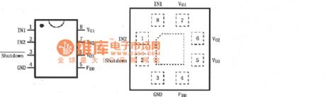
LM4910 is an audio power amplifier. It is primarily designed for portable devices, and it uses 3.3V power supply. It can output 35mW continuous average power todriver 32Ω load. LM4910 uses new topology circuit to cancle headphone amplifier output coupling capacitor and half-supply bypass capacitor, and it includes an advanced click - flutter noise elimination circuit. This noise generates instantly when you switch it off. LM4910 pinout is shown as the chart.
(View)
View full Circuit Diagram | Comments | Reading(986)
LM4809, LM4810 typical circuit diagram for two-channel headphone amplifier
Published:2011/8/31 2:34:00 Author:Rebekka | Keyword: two-channel headphone amplifier, typical circuit
Left and right channel audio signals are input M4809/4810(SOP/MSOP packaging) 2, 6 feet respectively. They are output by 1, 7 feet after being amplified by the internal amplifier. They will be added to the respective channel speaker through coupling capacitor. Amplifier gain Av = Rf / Ri. LM4809's pin 5 is connected externalshutdown control. when pin 5 is connected to VDD(high level), it is allowed to work; when pin 5 is grounded(low level), it can not work.
(View)
View full Circuit Diagram | Comments | Reading(1927)
LM4809, LM4810 Dual-channel headphone amplifier circuit diagram
Published:2011/8/31 2:35:00 Author:Rebekka | Keyword: Dual-channel , headphone amplifier
LM4809/4810 is dual channel headphone amplifier with 5V power supply. Each channel can output 105mW continuous average power to drive 16Ω load. Total harmonic distortion plus noise (THD + N) is only 0.1%. LM4809/4810 isthe minimum number of external components, which canprovide high-quality output power. LM4809/4810 does not require bootstrap capacitor and buffer. It is qualified to low-power portable systems. LM4809/4810 has an external control terminal to produce effectivelow level shutdown mode to work in the micro-power. There is an internal thermal shutdown protection agency. The pinout is shown as the chart.
(View)
View full Circuit Diagram | Comments | Reading(1230)
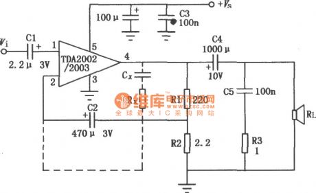
TDA2002, TDA2003 8W Audio power amplifier circuit diagram
Published:2011/8/31 2:35:00 Author:Rebekka | Keyword: 8W , Audio power amplifier
View full Circuit Diagram | Comments | Reading(3846)
TDA1512, TDA1512Q 20WHi-Fi audio power amplifier circuit diagram
Published:2011/8/31 2:36:00 Author:Rebekka | Keyword: 20WHi-Fi , audio power amplifier
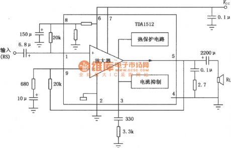
View full Circuit Diagram | Comments | Reading(2457)
Gain programmable low noise differential amplifier circuit composed of OPA37
Published:2011/8/31 2:38:00 Author:Rebekka | Keyword: Gain programmable low noise, differential amplifier
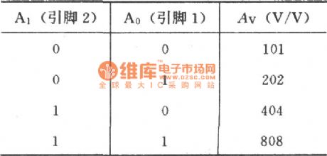
Total gain Av and A0, A1 corresponding relation:
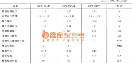
The main parameters of the OPA27 integrated chips (typical values):
The figure shows the gain programmable low noise differential amplifier circuit. The circuit is composed of two parts: The first level differential input consists of the two pieces of OPA27 high precision low noise op-amps , the second level is composed of the numerical control gain programming instrument amplifier PGA203.
(View)
View full Circuit Diagram | Comments | Reading(766)
LM2002, LM2002A 8W Audio power amplifier circuit diagram
Published:2011/8/31 2:41:00 Author:Rebekka | Keyword: 8W , Audio power amplifier
LM2002/2002Ais theaudio power amplifier IC. It uses 5-pin single in-line plastic package. The features of the two ICs are large output power, less distortion, low noise, small number of external components, high input impedance, low noise of power shock etc. LM2002 has limiting current and thermal shutdown protection circuit; LM2002A has a high voltage protection. The maximum instantaneous power supply voltage is up to 40V. They are suitable for the audio power amplifier of car audio systems, ordinary portable or desktop recorder. The BTU circuit is shown as the chart. (View)
View full Circuit Diagram | Comments | Reading(1518)
The integrated circuit diagram of two-channel audio power amplifier
Published:2011/9/18 21:16:00 Author:Ecco | Keyword: Two-channel audio , power amplifier , integrated circuit
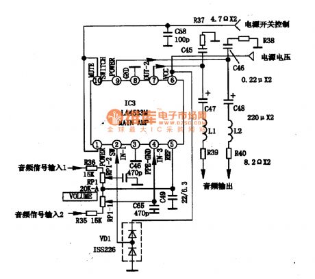

LA4533M is the two-channel audio power amplifier integrated circuit produced by Sanyo of Japan, and it is widely used in pocket radio, Walkman and other low-voltage, low-power audio system. 1. LA4533M internal block diagram and pin functions LA4533M manifold is mainly composed of two-way power amplifier circuit, power-off mute switch circuit, ripple filter circuit. The manifold internal block diagram is shown in Figure 1, the IC uses 10-pin dual flat plastic structure, and the integrated circuit pin functions and data are listed in Table 1.
(View)
View full Circuit Diagram | Comments | Reading(1502)
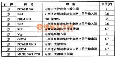
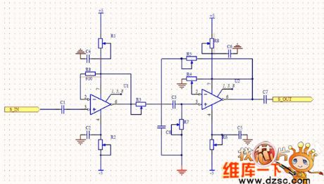
High-fidelity head amplification board circuit diagram
Published:2011/9/2 1:50:00 Author:Ecco | Keyword: High-fidelity head , amplification board
View full Circuit Diagram | Comments | Reading(886)
The amplifier circuit diagram with high-frequency power
Published:2011/9/9 2:08:00 Author:Ecco | Keyword: amplifier, high-frequency power
View full Circuit Diagram | Comments | Reading(740)
BoardBand Amplify circuit diagram
Published:2011/9/9 2:11:00 Author:Ecco | Keyword: BoardBand Amplify
View full Circuit Diagram | Comments | Reading(846)
Fever headphone amplifier circuit diagram 1
Published:2011/9/2 1:18:00 Author:Ecco | Keyword: Fever headphone amplifier
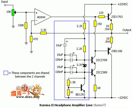
View full Circuit Diagram | Comments | Reading(1014)
Fever headphone amplifier circuit diagram 2
Published:2011/9/2 1:17:00 Author:Ecco | Keyword: Fever headphone amplifier
View full Circuit Diagram | Comments | Reading(1441)
Computer microphone principle diagram
Published:2011/9/9 2:06:00 Author:Ecco | Keyword: Computer microphone
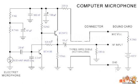
View full Circuit Diagram | Comments | Reading(897)
LM307, μA741 audio amplifier circuit diagram
Published:2011/9/9 1:58:00 Author:Ecco | Keyword: audio amplifier
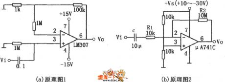
View full Circuit Diagram | Comments | Reading(1766)
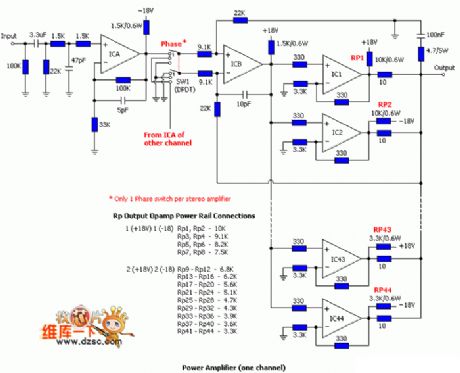
20KW Super amplifier circuit diagram
Published:2011/9/9 1:55:00 Author:Ecco | Keyword: 20KW Super amplifier
View full Circuit Diagram | Comments | Reading(4369)
| Pages:56/250 At 204142434445464748495051525354555657585960Under 20 |
Circuit Categories
power supply circuit
Amplifier Circuit
Basic Circuit
LED and Light Circuit
Sensor Circuit
Signal Processing
Electrical Equipment Circuit
Control Circuit
Remote Control Circuit
A/D-D/A Converter Circuit
Audio Circuit
Measuring and Test Circuit
Communication Circuit
Computer-Related Circuit
555 Circuit
Automotive Circuit
Repairing Circuit