
Amplifier Circuit
Index 50
Operational amplifier attenuation circuit diagram
Published:2011/8/19 2:15:00 Author:Jessie | Keyword: Operational amplifier, attenuation
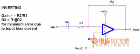
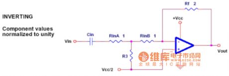
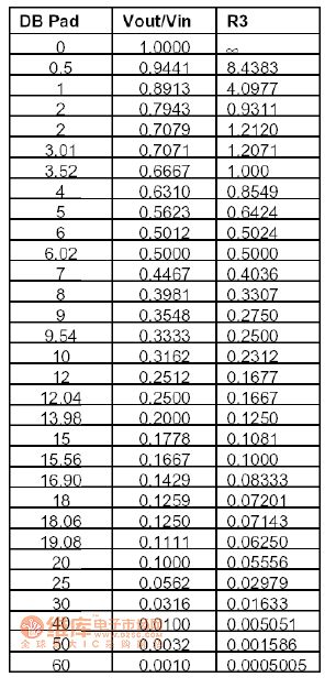
Reversed-phase composedof op-amp attenuator is shown in figure 1 . In the circuit, R2 is less than R1. This method is not recommended, because many op-ampsare not suitable for the working condition ofthe magnification whichis less than 1. Accurate method is to use figure 2 circuit. In table 1, a set of normalization of R3 resistor can be used to produced different level attenuation. The other resistors can use the following formula: R3=(Vo/Vin)/(2-2(Vo/Vin)). (View)
View full Circuit Diagram | Comments | Reading(1207)
YS-608 Learning headset principle and maintenance circuit
Published:2011/8/24 2:30:00 Author:Jessie | Keyword: Learning headset, principle, maintenance
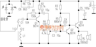
The headset circuit entirely composedof division components. When single pole double throw switch K is dialled to 1 position, the headset is at the state ofreceiving infrared, thereceiver tube will receive infrared speech signal from 100 parallel infrared emitting tubes which are in the back of the classroom. This signal is coupledfrom the capacitor C1 to Q1 to amplify, then the voice signal issent to the two level percentile amplifier circuit which is composedof Q2, Q3, and promote left/right two parallel headsets togive off sound. (View)
View full Circuit Diagram | Comments | Reading(851)
Operational amplifier virtual earth circuit
Published:2011/8/24 2:29:00 Author:Jessie | Keyword: Operational amplifier, virtual earth
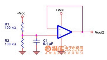
The op-amp of single-voltage's work requires to provide a virtualfor external, of whichvoltageisnormally VCC/2. In graph 2, thecircuit can be used to produce the VCC/2 voltage, butit will reduce the system frequency characteristics. R1 and R2are equivalent, which is choosen through the consumption and noise, and capacitorC1 is a low-pass filter, which is used to reduce the noise coming from power. In some applications,buffer op-amp can be ignored. (View)
View full Circuit Diagram | Comments | Reading(1161)
High-efficiency high power amplifier RF2131 pin circuit diagram
Published:2011/10/24 2:06:00 Author:May | Keyword: High-efficiency, high power, amplifier
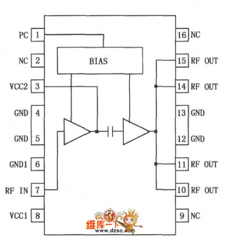
RF2131 is high-power and high-efficiency amplifier. It adopts advanced GaAs hetero-junction bipolar transistor technology. It is designed for final linear RF amplifier of ETACS handheld device, CDPD, band spread system and other applications with working frequencyin 1800~2500MHz. It offers an analog voltage input end with power control rangein 30dB. The power supply decreases when it is in the logic low-level state. And, the power supply is in the spare working state. It is designed for C class, but it can work at linear AB class if itimprove bias voltage. The device itself includes 50Ω input and output. So it is very easy to match best power and efficiency features. RF2131 is used for AMPS/ETACS cellular system mobile phone, CDPD portable data card, 900MHz ISM frequency range device, commercial and consumer systems, portable battery power supply unit, etc. The pin array of RF213 is shown in the diagram.
(View)
View full Circuit Diagram | Comments | Reading(1021)
The best efficiency power amplification circuit of RF2131 with 4.8V power
Published:2011/10/24 2:39:00 Author:May | Keyword: best efficiency, power amplification , 4.8V power
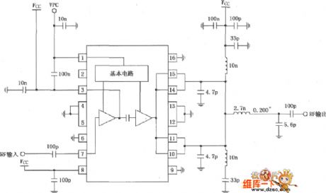
RF signal (RF) is input by pin 7, and it is output by pin 10, 11, 14 and 15 after enlarging by preamplifier and final stage power amplifier. Pin 7 is directly coupled with internal amplifier. So pin 7 is added a blocking coupling capacitor. The input impendence of pin 7 is 50Ω, but the precise resistance is determined by out connected internal matching network of pin 3. Pin 10, 11, 14 and 15 of output endare connectedto the chip. Normally, pin 10. 11, 14 and pin 15are separately connected together and used as signal output.People must pay attention to symmetry. In order to get largest output power and efficiency, output matching network can make amplifier's output impendence match with it. At the same time, the pins are also used as final power amplifier's power supply end. It offers bias current to final operation amplifier through the pins. (View)
View full Circuit Diagram | Comments | Reading(836)
RF2132 Dual-mode high-power linear amplifier pin diagram
Published:2011/10/24 2:42:00 Author:May | Keyword: Dual-mode, high-power, linear amplifier
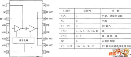
RF2132 is a high power and efficiency linear amplifier. It is treated by advanced GaAs hetero-junction bipolar transistor. And it is designed for the final linearity RF amplification of double mode four battery's CDMA/AMPS handheld digital cellular system equipment, band spread system and other applications with working frequency 800~950MHz. The device itself includes 50Ω input and output. So it is very easy to match and get best power, efficiency and linear property when the whole power supply and control voltage changes. FR2132 is used in 4.8V AMPS cellular systems mobile phone, CDMA/AMPS mobile phone, JCDMA/TACS mobile phone. It can also beused as driver amplifier, portable battery supplyin the base station. The pin array and functions of RF2132are shown in the diagram.
(View)
View full Circuit Diagram | Comments | Reading(949)
Linear power amplifier circuit composed of RF2132
Published:2011/10/24 2:50:00 Author:May | Keyword: Linear power amplifier
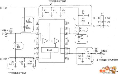
The diagram is linear power amplifier circuit composed of RF2132. Radio-frequency signal (RF) isinput by pin 3, enlarged by preamplifier and final power amplifier, then output by pin 10, 11. Pin 3 is directly coupling with internal amplifier, and it is added a blocking coupling capacitor, and the input resistance of pin 3 is 50Ω, but the precise resistance is determined by interstage matching network connected to pin 1. L1 is output center frequency level adjusting inductance; R1 can improve linearity, add first level ampliifer current bias; L2 is amplifier output stage bypass inductor. Output ends pin 10, 11, 14, 15 are connected to the chip. Pin 8 is connected topower control foot (PC) to control this pin voltage and power. At room temperature, when voltage is inlow level ( when it is 0.5V or lower) , amplifier power is on the shutoff state. Vcc=4.8V, Vpc=4.0V.
(View)
View full Circuit Diagram | Comments | Reading(1236)
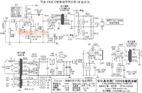
T1A-14 vacuum tube one-port class A amplifier-headphone amplifier amphibious circuit
Published:2011/8/29 20:57:00 Author:Jessie | Keyword: vacuum tube, one-port class A amplifier, headphone amplifier, amphibious circuit
View full Circuit Diagram | Comments | Reading(2881)
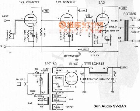
2a3 tube amp circuit diagram
Published:2011/8/29 21:17:00 Author:Jessie | Keyword: tube amp
View full Circuit Diagram | Comments | Reading(3444)
Bravery machine amplifier pins circuit diagram
Published:2011/8/24 2:39:00 Author:Jessie | Keyword: Bravery machine, amplifier pins
View full Circuit Diagram | Comments | Reading(740)
Banqiu HE-2700E1, HE-2700E2 temperature-regulating electric furnace circuit diagram
Published:2011/8/29 22:37:00 Author:Jessie | Keyword: Banqiu, temperature-regulating , electric furnace
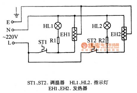
ST1, ST2-thermostat, HL1.HL2-light, EH1, EH2 heater
(View)
View full Circuit Diagram | Comments | Reading(793)
Meifeng DYB40-80A insulation automatic electric pressure cooker circuit
Published:2011/8/24 2:37:00 Author:Jessie | Keyword: insulation, electric pressure cooker
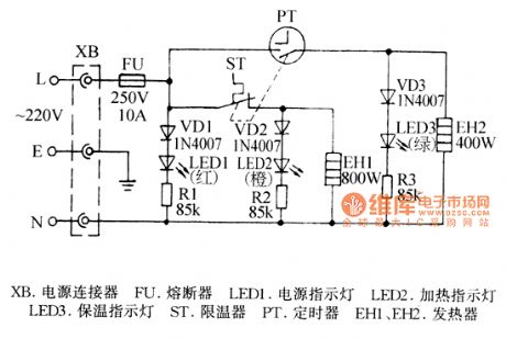
XB-power connector, FU-fuse, PT-timer,EH1,EH2-heater,led1-power indicator, LED2-heater indicator, LED3-heater lamp (View)
View full Circuit Diagram | Comments | Reading(779)
Jiabao YWB-55 automatic electric pressure cooker circuit
Published:2011/8/24 2:33:00 Author:Jessie | Keyword: electric pressure cooker
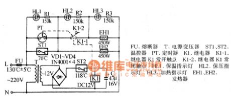
FU-Fuse, T-power transformer, ST1, ST2-thermostats, PT-timer, K1-relay, K1-1 normally open contact of relay K1, K1-2-relay normally closed contact of K1, HL1-heat indicator, EH1, EH2-heaters (View)
View full Circuit Diagram | Comments | Reading(1205)
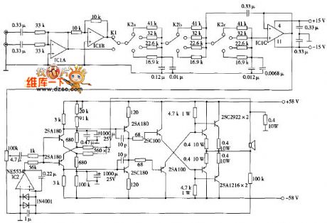
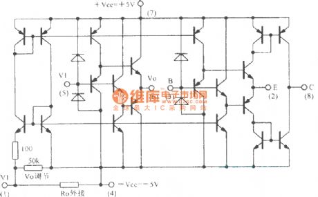
Active servo power amplifier circuit for lifting subwoofer
Published:2011/12/8 20:46:00 Author:Ecco | Keyword: Active servo , power amplifier , lifting subwoofer
View full Circuit Diagram | Comments | Reading(3371)
8W amplifier
Published:2011/12/6 1:37:00 Author:Ecco | Keyword: 8W , amplifier
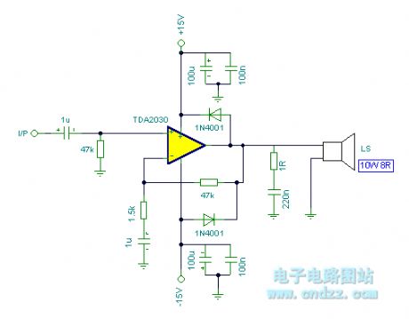
Although the TDA2030 can deliver 20 watts of output power, I deliberately reduced the output power to about 8 watts to supply 10 watt speakers. Input sensitivity is 200mV. Higher input levels naturally will give greater output, but no distortion should be heard. The gain is set by the 47k and 1.5k resistors. The TDA2030 IC is affordable and makes a good replacement amplifier for low to medium audio power systems. Incidentally, it is speaker efficiency that determines how 'loud' your music is. Speaker efficiency or sound pressure level (SPL) is usually quoted in dB/meter. A speaker with an SPL of 97dB/m will sound louder than a speaker with an SPL of 95dB/m.
(View)
View full Circuit Diagram | Comments | Reading(1045)
CA3080 variable gain amplifier circuit
Published:2011/12/6 20:26:00 Author:Ecco | Keyword: variable gain , amplifier
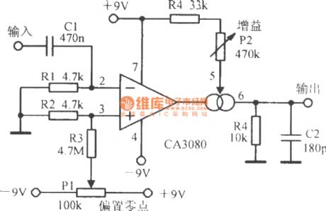
View full Circuit Diagram | Comments | Reading(2607)
15W amplifier
Published:2011/12/6 1:42:00 Author:Ecco | Keyword: 15W , amplifier
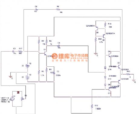
This amplifier uses a dual 20 Volt power supply and delivers 15 watts RMS into an 8 ohm load. Q1 operates in common emitter, the input signal being passed to the bias chain consisting of Q8, Q9, D6, D13 and D14. Q8 and Q9 provide a constant current through the bias chain to minimize distortion, the output stage formed by a discrete darlington pair (Q2,Q4) and (Q7,Q11). The last two transistors are power Transitors, specifically the 2N3055 and MJ2955. The 7.02K resistor, R16 was made using a series combination of a 4.7K, 680 Ohms, and two 820 Ohms. The 1.1K resistor, R3 was made using a 100 Ohms and a 1K resistor. You can use this circuit with any walkman or CD player since it is designed to take a standard 500mv RMS signal.
(View)
View full Circuit Diagram | Comments | Reading(1052)
Broadband operational amplifier
Published:2011/12/5 21:25:00 Author:Ecco | Keyword: Broadband , operational amplifier
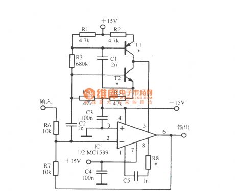
View full Circuit Diagram | Comments | Reading(865)
Wideband operational transconductance amplifier buffer circuit OPA660
Published:2011/12/5 21:24:00 Author:Ecco | Keyword: Wideband , operational, transconductance, amplifier, buffer
The internal principle circuit:
(View)
View full Circuit Diagram | Comments | Reading(1904)
Zero-drift inverting amplifier circuit
Published:2011/12/5 21:15:00 Author:Ecco | Keyword: Zero-drift , inverting amplifier
View full Circuit Diagram | Comments | Reading(737)
| Pages:50/250 At 204142434445464748495051525354555657585960Under 20 |
Circuit Categories
power supply circuit
Amplifier Circuit
Basic Circuit
LED and Light Circuit
Sensor Circuit
Signal Processing
Electrical Equipment Circuit
Control Circuit
Remote Control Circuit
A/D-D/A Converter Circuit
Audio Circuit
Measuring and Test Circuit
Communication Circuit
Computer-Related Circuit
555 Circuit
Automotive Circuit
Repairing Circuit