
Amplifier Circuit
Index 44
200W audio amplifier circuit
Published:2012/10/9 2:42:00 Author:muriel | Keyword: 200W, audio amplifier
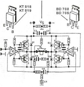
This audio amplifier circuit delivers up to 200 W of top-class quality for loudspeaker from 4 to 16 ohm. Operating voltage is between 24 and 36 V, max 5 A. The frequency response is from 20 to 20000 Hz.Please take special care that the transistors and the IC’s have been fixed firmly and solely one or two separated cooling elements with sufficient dimensions for this purpose (thermal resistance < 1K/W).
200W Power Amplifier circuit diagram
Doing so it is necessary to mount the transistors and the IC’s insulated (with mica washes and plastic nipple). Please make sure before first operation that the transistors and the IC’s really do not have any electrical connection towards the cooling plate! The transistors have to be placed plane and firmly onto the cooling element! It is of extraordinary importance with this high-power amplifier that there is a considerable heat dissipation. The already mounted cooling element should be situated in a well ventilated case.
The PSU should be sufficiently powerful, power consumption of the amplifier may increase up to 5A. In case of using an unstabilised power supply. It is advisable to place a transformer of max 28V.
The amplifier will the show approx. 120W at a 4-Ohm loudspeaker, for it no-load voltage of the power supply will not be to high. If it is desired to use complete power, it is necessary to place a stabilised power supply with approx. 36V 5A. No-load voltage should not pass over 44V!The cables leading the current supply and to the loudspeakers should have at least a cross section of min. 1.5 mm^2. The connected loudspeaker have to be equiped according to the high output power and should not have a lower impedance as 4 Ohm! With lower connection impedance and short circuit within the loudspeaker wiring, the transistors will be destructed.
The amplifier has an input sensitivity of approx. 500 … 800 mV. Therefore, it is possibile to connect directly at the amplifier tape decks, tuners, etc. In case there are connected signal sources with lower output voltage, it is necessary to pre-connect a preamplifier. Then it will alse be posible to connect microphones, etc.
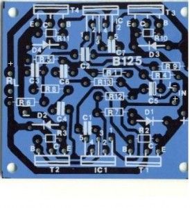
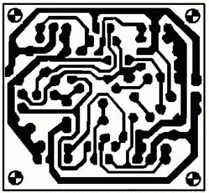
200W audio amplifier PCB
(View)
View full Circuit Diagram | Comments | Reading(1527)
VMOS 144 MHz Push Pull DV28120T amplifier
Published:2012/10/9 2:41:00 Author:muriel | Keyword: 144 MHz, Push Pull, DV28120T, amplifier
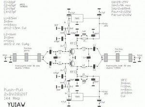
This is a 2 meters 144 Mhz rf amplifier wich works in push pull and is build with DV28120T Vmos.You can use coils made form RG142 coaxial cable or similar, 620mm long , 5mm diameter, 6 turns with inside diameter 30mm no gaps between.
VMOS RF amplifier circuit diagram
(View)
View full Circuit Diagram | Comments | Reading(1412)
TDA2822 Stereo Amplifier Circuit
Published:2012/10/9 2:40:00 Author:muriel | Keyword: TDA2822, Stereo Amplifier
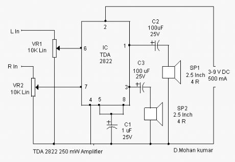
TDA2822 is a low power stereo Op Amp used in Walkman players and Hearing aids. It can give 250 milli watts output. TDA2822 is an ideal Op amp for low output applications. It is a good choice as a preamplifier in stereo high power amplifier circuits. It has two inputs and two outputs which can deliver 250 milli watts output power. The amplifier circuit with in the IC is well set for noise free operation. Outputs can be directly coupled to the speakers through the decoupling capacitors.
TDA2822 amplifier circuit diagram
(View)
View full Circuit Diagram | Comments | Reading(2596)
Transistor Amplifier Design
Published:2012/10/8 2:36:00 Author:muriel | Keyword: Transistor Amplifier
Good stability and sufficient amplification in Transistor based circuits depends on the proper selection of components and their layout. Gain of the transistor used as well as the current and voltage through it are the most important aspect in the working of a transistor amplifier. Here explains the design parameters of an one transistor amplifier circuit. Circuit layout of the Transistor Amplifier
A PNP signal amplifier is shown in Fig.1. It is used to amplify the signals using a PNP transistor. Resistors are placed in their positions but values are not fixed. The resistors around T1 includes
1. R2-R1- A potential divider to provide base current to T1.2. R3 – Emitter resistor of T1 that determines the Emitter voltage and current.3. R4 –Collector resistor of T1 that determines the collector voltage and current and hence the strength of output signal.
Fig.1 Transistor Amplifier Layout (View)
View full Circuit Diagram | Comments | Reading(1134)
FET Preamplifier circuit
Published:2012/10/8 2:35:00 Author:muriel | Keyword: FET Preamplifier
Field Effect Transistor is an amplifying device in which the output current depends on the input voltage. The FET Pre Amplifier described here is a sensitive and stable Preamp circuit using an N-Channel FET and a PNP Bipolar transistor. This combination gives high input impedance and low output impedance with stabilized gain. The Junction FET has a conducting channel .It’s one end is the Source and the other end is Drain. The junction FET has direct ohmic contact at the gate. The enclosing material forms the Gate. If the channel is formed of N- material and the gate is formed of P -material, the FET is called as N-channel FET. If the arrangement is of the opposite type, then it is called as P-channel FET. The conductance of the channel can be controlled by the Gate-Source potential and then current flows from drain to source.
FET Pre Amp Circuit diagram
BFW11 DatasheetThe circuit is a sensitive preamplifier using an N-Channel FET and a PNP transistor. This combination gives high input impedance and low output impedance with stabilized gain. Any general purpose PNP transistors like BC 557 or BC558 can be used according to the required gain. The gain of the Preamp depends on the Feedback network and with the given values of R4 and R5, it is around 20. Input of the preamp is sensitive and readily matches with microphones and ceramic pick up. (View)
View full Circuit Diagram | Comments | Reading(1029)
IC CA3140 datasheet
Published:2012/9/27 21:22:00 Author:muriel | Keyword: CA3140
CA3140 is the 4.5MHz BiMOS Operational Amplifier with MOSFET inputs and Bipolar output. This Op Amp combines the advantage of PMOS transistors and high voltage bipolar transistors.
CA3140 has gate protected MOSFETs (PMOS) transistors in the input circuit to provide very high input impedance typically around 1.5T Ohms.The IC requires very low input current as low as 10pA to change the output status, high or low. The IC has very fast response and high speed of performance. The output stage of the IC uses bipolar transistors and includes built in protection against damage from load terminal short circuiting to either supply rails or to ground.
The use of PMOS FET in the input stage results in common mode input voltage capabilities down to 0.5 volts below the negative supply terminals. These operational amplifiers are internally phase compensated to achieve stable operation in unity gain follower operation, and additionally, have access terminal for a supplementary external capacitor if additional frequency roll-off is desired. Terminals are also provided for use in applications requiring input offset voltage Nulling.
Pin connectionsThe CA3140 Series has the same 8-lead pin out
Pin1Offset NullPin2 Inverting input INVPin3 Non inverting input Non-INVPin4 Ground- Negative supplyPin5 Offset NullPin6 OutputPin7 Positive supplyPin8 Strobe
Operating conditions
Supply voltage 36 volt maximumInput terminal current 1mA
CA3140 Block Diagram
Nulling of Offset Voltage
The input offset voltage can be nulled by connecting a 10K pot between the terminals 1 and 5 and returning its wiper to the ground. This technique, however, gives more adjustment range than required and therefore, a considerable portion of the potentiometer rotation is not fully utilized. (View)
View full Circuit Diagram | Comments | Reading(1593)
Recording head amplifier circuit
Published:2012/9/24 22:14:00 Author:Ecco | Keyword: Recording head amplifier
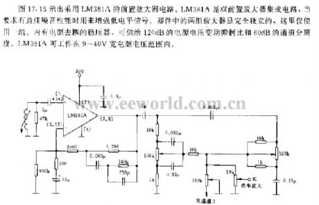
The preamplifier circuit using LM381A is shown in Figure 17.15. LM381A is a dual preamplifier IC which is used to enhance the low-level signal when it is required optimum noise performance. Two sets of amplifier devices are completely independent, the circuit here only uses one group. It contains the power supply decoupling regulator to provide 120dB power supply voltage variation rejection ratio and 60dB channel separation. LM381A can work in wide power supply voltage with range in 9 ~ 40V.
(View)
View full Circuit Diagram | Comments | Reading(1364)
The particular application circuit of op amp
Published:2012/9/23 21:51:00 Author:Ecco | Keyword: particular application , op amp
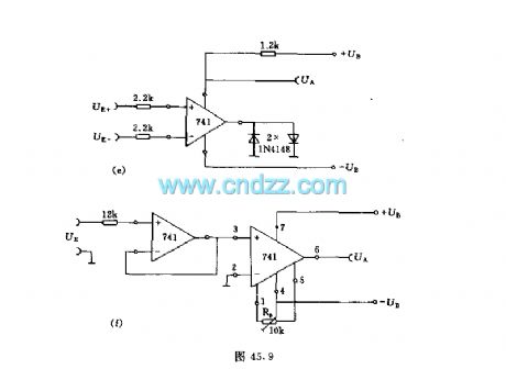
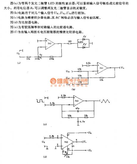
Figure A is polarity display with two light emitting diodes, and it can be used to idendify the input signal polarity or the size of comparison signal. It uses potentiometer RP to adjust the display sensitivity oftwo light-emitting diodes.The circuit shown in figure b is used for adding several input signals UE1.UE2 and UE3.The circuit shown in Figure is a precision integrator circuit, and its RC network must match the input signal.Figure d shows a comparator circuit.The Figure e is the comparator circuit with higher frequency and the symmetrical input.Figure f is the precision comparator circuit with the voltage follower at the input termination.
(View)
View full Circuit Diagram | Comments | Reading(897)
Automatically polarity selecting electric E amplifier circuit
Published:2012/9/23 21:41:00 Author:Ecco | Keyword: Automatically , polarity selecting, electric E , amplifier
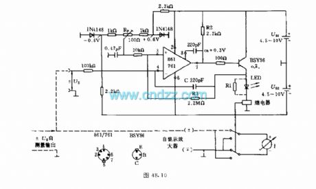
The measured voltage conversion by change-over switch is time consuming, and it is easy to generate mistake. The circuit shown in figure uses relays to automatically convert polarity. The operational amplifier 861 or 761 is used as comparator. The output voltage can control relay by the emitter follower. The relay coils is connected with a light emitting diode in series to display the selected signal.
(View)
View full Circuit Diagram | Comments | Reading(2831)
LM317 audio amplifier
Published:2012/9/24 4:06:00 Author:muriel | Keyword: audio, amplifier
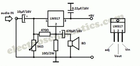
You probably know that LM317 IC is used as an adjustable voltage regulator, but did you know it can be used as an audio amplifier? This is a class A audio amplifier built with LM317 that delivers a maximum 1W audio power.
Use a good heatsink for the LM317 IC and adjust the 5K variable resistor so that you have 4.5V on 10Ω resistor (or LM317 pin 2, Vout).
LM317 amplifier schematic
Source: vegmatic1966′s Youtube Channel
Video explanation of the working principle
?
19 Responses to “LM317 audio amplifier”
(View)
View full Circuit Diagram | Comments | Reading(2958)
The amplifier circuit with macroaxis and low current
Published:2012/9/20 22:00:00 Author:Ecco | Keyword: amplifier , macroaxis, low current
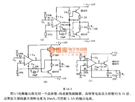
Figure A shows the amplifier circuit using a high-output-power and small-distortion complementary transistor. Two diodes can significantly reduce the controlling dead zone. The emitter of two transistors is connected to a strong negative feedback, the dead zone can be further reduced.The circuit shown in Figure b is simpler than the circuit shown in Figure a, and it also uses strong negative feedback to reduce the dead zone.The output stage of circuit shown in Figure c only uses one transistor to form a emitter follower. The transistor current magnification is about 75 times. The op amp maximum current consumption is 20mA to control 1.5A output current.
(View)
View full Circuit Diagram | Comments | Reading(1376)
Pre-amplifier circuit with a high input resistance
Published:2012/9/20 21:46:00 Author:Ecco | Keyword: Pre-amplifier , high input resistance
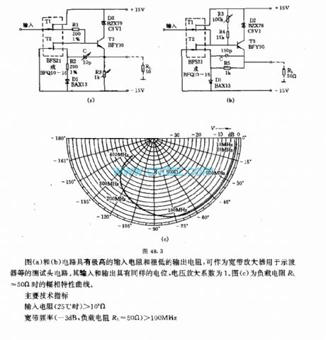
The circuits shown in Figures a and b have a high input resistance and low output resistance, and they can be used as a broadband amplifier for oscilloscopes and other test head circuits. Their input and output have the same potential, the voltage amplification factor is 1. Figure c shows the amplitude and phase characteristic curve when the load resistance RL = 50Ω.The main technical indications:Input resistance (25 ℃ pm ) > 10 9 ΩBroadband frequency (-3dB, load resistor RL = 50 Ω ) > 100MHzOutput resistance of < 10 Ω
(View)
View full Circuit Diagram | Comments | Reading(1332)
Selective amplifier circuit
Published:2012/9/20 21:38:00 Author:Ecco | Keyword: Selective amplifier

The general selective amplifier uses double T network which requires high-precision component parameters. But the circuit shown in Figure can avoid the question. The frequency f0 is determined by C1 at low pass and C2 at high pass.
(View)
View full Circuit Diagram | Comments | Reading(995)
Output power amplifier circuit of operational amplifier
Published:2012/9/20 1:08:00 Author:Ecco | Keyword: Output power amplifier, operational amplifier
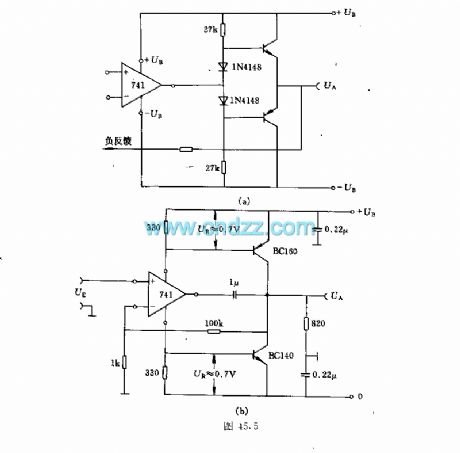
The circuit shown in Fig uses two transistors as an emitter follower, and diode for reducing the control dead zone (transistor base - emitter voltage UBEs = 0.7V ), and about 1mA current on the base resistor to form a bias and decide electrode quiescent current. The circuit shown in Figure b is connected to two resistors in the op-amp power connection. The quiescent current from two resistors flowing through the operational amplifier to produce about 0.7V voltage drop.
(View)
View full Circuit Diagram | Comments | Reading(1373)
The broadband amplifier circuit with 600v/us conversion speed
Published:2012/9/20 0:47:00 Author:Ecco | Keyword: broadband amplifier , 600v/us, conversion speed
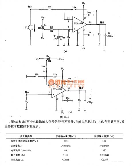
The circuits shown in Figures a and b have different signs of the input signal and input impedance Ze, and the main technical data is shown in the following table.
(View)
View full Circuit Diagram | Comments | Reading(1114)
Wideband op amp circuit
Published:2012/9/19 22:51:00 Author:Ecco | Keyword: Wideband op amp
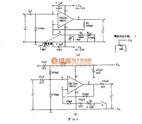
The circuit shown in Figure has overload protection measures. When the circuit has DC-coupled input, the input terminal can be connected to RC blocking network. When the switch S is opened, voltage amplification factor Ku = 1 ( voltage follower ). When S is closed, Ku = 10. For example, R1 = 100kΩ, R2 = R1 / ( Ku- 1 ) = 100/ 9 = 11.1kΩ. R2 = 10kΩ, the circuit is connected to a 2.5kΩ potentiometer Rp in series. The circuit shown as Figure b uses 10 ~ 20V voltage source, this input terminal is connected to a voltage divider.
(View)
View full Circuit Diagram | Comments | Reading(1137)
The terminal and internal function of operational amplifier
Published:2012/9/20 1:14:00 Author:Ecco | Keyword: terminal , internal function , operational amplifier
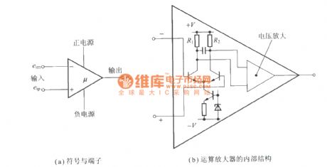
Figure a shows the signs and terminals.
Figure b shows the internal structure of operational amplifier.
(View)
View full Circuit Diagram | Comments | Reading(878)
3 band equalizer circuit
Published:2012/9/19 21:22:00 Author:Ecco | Keyword: 3 band, equalizer
This 3 band equalizer circuit is an active filter network for bass, mid and high audio ranges. It is designed around the LM833 opamp from National Semiconductors.This opamp IC has the following charactersistics: very low noise figure, wide bandwidth and a relatively high slew rate. How does the three band audio equalizer works
The output of this 3 way graphic equalizer is designed to be DC coupled, however due to slight DC variations through the 100K potentiometers at the feedback lines of the opamp A2, a coupling capacitor might be needed.
Technical specifications for the 3 band equalizer
The cutoff frequencies:
bass range = 200 Hz
high range = 2 kHz
The midrange is a bandpass network with a center frequency of 1 kHz.The maximum equalizer range is about 15 dB. In the middle position of potentiometer, the noise attenuation is about 90 dB with a bandwidth of 1 MHz and a gain of 0 dB. The gain can be changed through R2 using the following formula: Vu = R2/R1.
Audio Equalizer Circuit Diagram
?
No Responses to “3 band equalizer circuit”
Source: electroschematic.com
(View)
View full Circuit Diagram | Comments | Reading(944)
USB Power Booster
Published:2012/9/18 21:33:00 Author:Ecco | Keyword: USB, Power Booster
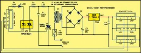
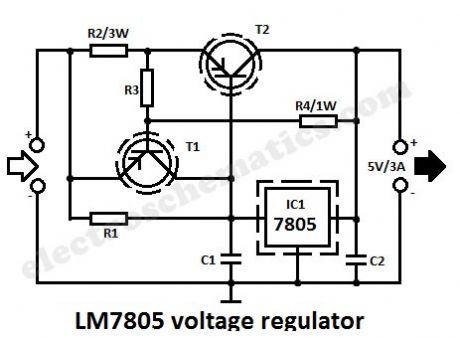
As you probably know, the USB 2.0 ports can deliver up to 500 mA, that means about 2.5W. But sometimes you might need more power to connect an external HDD or other peripherals and the USB ports just cannot deliver enough current. In this case you can buy USB hubs that have an external power adapter required to boost the power or you can build a simple or complex circuit that can do the same thing.
There are many usb power booster projects available on the internet, some of them are very complicated, others are simple as using a few components. One simple design involves the use of the 7805 voltage regulator that can deliver 5V and 1A.
Circuit No 1I have found this design on Electronics For You website and it uses the 7805 regulator, a MOC3021 optoisolator as main components. (source)
Circuit No 2This is another design that uses LM2575-5 step-down switching voltage regulator. Its principle is that internal power transistor switch on and off according to a feedback signal. This chopped or switched voltage is converted to DC with a small amount of ripple by D1, L1 and C2.
Circuit No 3This usb power booster circuit is the simplest one and it uses the 7805 voltage regulator that can deliver up to 1A.
Circuit No 4It uses the same 7805 but with 2 external transistor it can deliver up to 3 amps, that is 15W of power (source).
Of course you will need an external adapter to power up this circuits, something like a 12V DC adapter. What do you think?
Source: electroschematics.com
(View)
View full Circuit Diagram | Comments | Reading(1887)
How to move a trip point of Op-Amp comparator Circuit
Published:2012/9/18 21:29:00 Author:Ecco | Keyword: How to move , trip point , Op-Amp comparator

You all will be?familiar of basic comparator using a Op-Amp circuit. So today we will show you how to move a trip point of a Op-Amp comparator circuit. Maybe many of people already know this, but still this is the post for?beginners. So if you already know quit reading now only.
As shown in the above circuit, by application of a reference voltage to the inverting input rather than grounding it the trip can be moved. The reference voltage is given to the inverting input of a basic comparator using a potential divider consisting of resistors R1 and R2. The reference voltage Vref is derived using +Vcc and potential divider R1 and R2. Mathematically Vref is expressed as,
Vref = [+Vcc/(R1+R2)] R2
Now as long as the input voltage is less than Vref, the output is low i.e. -Vsat. When Vin becomes slightly greater than Vref, the Op-Amp output becomes high i.e. +Vsat. Thus the trip point is moved from Vin = 0 to Vin = Vref due to reference voltage applied to the inverting input terminal.
A bypass capacitor is used on the inverting input to reduce the amount of power supply ripple and noise appearing at the inverting input of Op-Amp. For effective bypassing of ripple and noise, the critical frequency of bypass circuit must be much lower than the ripple frequency of power supply.
The transfer characteristics of such a comparator is shown in above diagram which indicates positive trip point. Such a comparator is also called a limit detector as it detects the particular positive level of the input beyond which input goes high. The resistance R1 and R2 can be used to set the trip point anywhere between 0 and +Vcc.
The cut-off frequency of bypass circuit is,
fc = 1/[ 2π(R1||R2) Cby.
This must be much lower than the ripple frequency of the supply.10 Responses to “How to move a trip point of Op-Amp comparator Circuit?”
(View)
View full Circuit Diagram | Comments | Reading(864)
| Pages:44/250 At 204142434445464748495051525354555657585960Under 20 |
Circuit Categories
power supply circuit
Amplifier Circuit
Basic Circuit
LED and Light Circuit
Sensor Circuit
Signal Processing
Electrical Equipment Circuit
Control Circuit
Remote Control Circuit
A/D-D/A Converter Circuit
Audio Circuit
Measuring and Test Circuit
Communication Circuit
Computer-Related Circuit
555 Circuit
Automotive Circuit
Repairing Circuit