
Amplifier Circuit
Index 54
The improving input impedance amplifier circuit with FET
Published:2011/11/3 3:00:00 Author:Ecco | Keyword: improving input impedance , amplifier circuit , FET
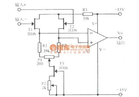
View full Circuit Diagram | Comments | Reading(984)
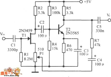
The basic circuit of differential amplifier
Published:2011/11/1 21:09:00 Author:Ecco | Keyword: basic circuit, differential amplifier
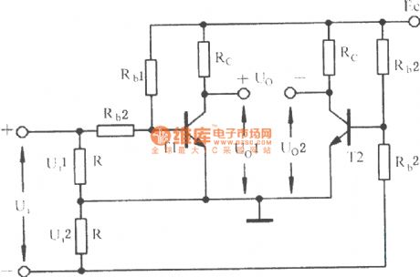
View full Circuit Diagram | Comments | Reading(1047)
Small FM transmitter ( wireless speaker) circuit
Published:2011/10/31 3:02:00 Author:May | Keyword: FM transmitter, wireless speaker
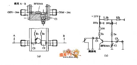
This circuit consists of transistor BFR34A,and the figure(a) shows its mechanical structure, when it worksat operating point, Uce=12V, Ic=17mA, theoutput power is12mW.Figure (b) is thebasic circuit. The collector's pins are grounded for better heatdissipation. The optimal phase condition of feedback between tmitter and collector isadjustedby coaxial wire. Variable output coupling capacitor is composed of the small thin plate with side length in5mm.
(View)
View full Circuit Diagram | Comments | Reading(2105)
VCA voltage control amplifier circuit diagram
Published:2011/10/18 3:47:00 Author:Ecco | Keyword: VCA , voltage control amplifier
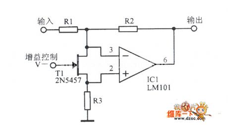
View full Circuit Diagram | Comments | Reading(4744)
The feedback amplifier circuit diagram
Published:2011/10/18 3:40:00 Author:Ecco | Keyword: Feedback amplifier
View full Circuit Diagram | Comments | Reading(1047)
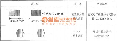
BL20106 infrared receiver preamplifier integrated application circuit diagram
Published:2011/9/27 1:59:00 Author:Rebekka | Keyword: infrared receiver preamplifier , integrated circuit
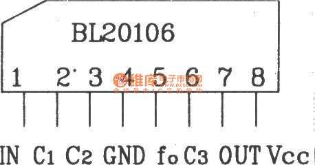
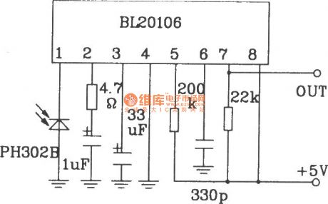

BL20106 is produced by Shanghai Belling Electronic Technology Co., Ltd. It is infrared remote control system for receiving bipolar preamplifier ASIC. Its features are: Low power consumption, low voltage, the internal band-pass filter everywhere; Output is an open collector output, and it can be connected with CMOS and TTL circuit; Input can be directly connected with the photodiode. Domestic and foreign similar products are D20106, CX20106, KA2184A and these can be directly interchangeable.
The figure below shows a typical application circuit constituted by the BL20106, andthe circuit is very simple, and its typical operating voltageis 4.7 ~ 5.3V, the circuit operating frequency is F0 = 40kHz
BL20106 shape pin map.
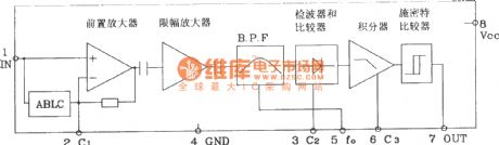
BL20106 internal block diagram.
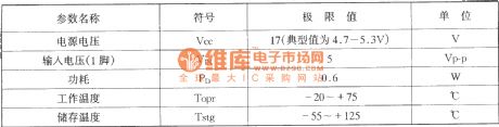
BL20106 limit of the operating parameters: (TA = 25 ℃)
BL20106 working waveform is shown as below:
(View)
View full Circuit Diagram | Comments | Reading(1274)
TDA2009 mono and stereo audio power amplifier circuit diagram
Published:2011/10/20 21:12:00 Author:Rebekka | Keyword: mono , stereo audio , power amplifier

Pin 1: 1.2V-- left channel input Pin 2: 0.8V-- left channel feedback Pin 3: 12V - Squelch Pin 4: 0.8V--right channel feedback Pin 5: 1.2V--right channel input
Pin 6: 0V - groundPin 7: 0V - empty Pin 8: 12.4V-- right channel outputPin 9: 24V - Power Pin 10: 12.4V-- left channel output (View)
View full Circuit Diagram | Comments | Reading(5054)
805 cathode follower direct coupling power amplifier circuit
Published:2011/10/24 2:15:00 Author:May | Keyword: cathode follower, direct coupling, power amplifier

The practical situation is: due to the push tube's cathode minimum voltage is 0V, the practical 805 grid push range only has 0V~45V, at this time, in theoperating point namely the small triangle area, output power P0'=0.5(1425-1050)/(100-55)*1000 = 8.5W.
This is the biggest shortcoming of this type circuit. For low sensitivity sound box, it will lead to clipping distortion to turn the volume up. It is clearly that it can negligent if you never turn up so big volume. But if it only outputs 8.5W, the operating factor is so low. And the better choice is to adopt 300B. It is hard to achieve without minus gate voltage part if you want to get higher output power. (View)
View full Circuit Diagram | Comments | Reading(2630)
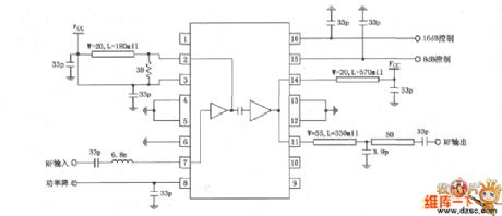
824~849MHz power amplifier circuit composed of RF2152
Published:2011/10/24 2:45:00 Author:May | Keyword: 824~849MHz, power amplifier
The diagram shows 824~849MHz power amplifier circuit composed of RF2152. Radio-frequency signal (RF) is input by pin 6, and it is output by pin 12 and 13 after enlarging by preamplifier and final amplifier. Pin 6 is directky coupling with internal amplifier, so it is added a blocking coupling capacitor in the pin 6. Output ends 12, 13, 14are connected to the chip, output matching network canmake amplifier output resistance match with it to get themaximum output power and efficiency. At the same time, pin 12, 13 are used as final power amplifier source supply's end, and it provides bias current through the pins.Pin 14 is used asthesecond harmonic's filter circuit. Pin 7 or 3 are connected to power control foot (PC) tocontrol this pin's voltage and source power. When voltage is inlow level (when 0.5V or lower), amplifier is in the offstate; when voltage is in high level (2.8V), amplifier power is in the standard working state. R3 and R4are usedfor bias adjustment.
(View)
View full Circuit Diagram | Comments | Reading(847)
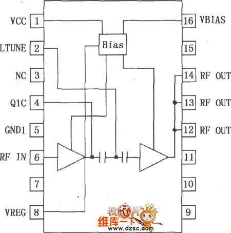
RF2155 programmable plus power amplifier pin circuit
Published:2011/10/23 22:50:00 Author:May | Keyword: programmable, plus, power amplifier
RF2155 is the programmable plus amplifier IC, and it is used in 3V handheld systems. It uses advanced GaAs heterojunction bipolar transistor (HBT), and it is designed for final linear RF amplification of analog cellular telephone system transmitter or applications with ISM working frequency 915MHz. Except outside match network, device itself includes power supply line. The two bits digital controlling offers 4 levels of power with 8dB per step. The pin array of RF2155 is shown in the diagram.
(View)
View full Circuit Diagram | Comments | Reading(943)
915MHz power amplifier application circuit composed of RF2155
Published:2011/10/24 1:23:00 Author:May | Keyword: 915MHz, power amplifier
The diagram is 915MHz power amplifier application circuit composed of RF2155. Radio-frequency signal (RF) is input by pin 7, then it is output by pin 11 after enlarged by preamplifier and final power amplifier. Pin 7 and internal amplifierare directly coupled. So it is advised to add UHF blocking coupling capacitorto the out end of pin 7. Final power amplifier is mismatching collector transistor, output end of pin 11 and pin 14 is connected inside of the chip, pin 14 is used as final power amplifier supply side, it offers bias current to final power supply. Pin 14 is also used as thesecond harmonics filter circuit. It uses about 500mils transmission line as inductance. Pin 8 connects to power control foot (PC), and it can control this pin voltage thus control power. When voltage is low( 0V), amplifier power is in the open state; when voltage is inhigh level (3V), amplifier is in the total power working state.
(View)
View full Circuit Diagram | Comments | Reading(1325)
RF2175 400MHz linear amplifier pin circuit
Published:2011/10/23 21:12:00 Author:May | Keyword: 400MHz, linear amplifier
RF2175 is high-power, high-performance linear amplifier IC which is applicated in 3V handheld systems, and ituses advanced GaAs heterojunction bipolar transistor ( HBT). It isintended for TERA handheld digital cellular system equipment's final stage linear RF amplification, band spread system and its working frequency is 380~512MHz. RF2175 has an analog bias control voltage to generate themaximal efficiency, and it includes 50Ω input and output, and it is easy to get best power, efficiency linear performance. RF2175 uses SSOP-16 plastic package, andits pin array is show in the diagram.
(View)
View full Circuit Diagram | Comments | Reading(936)
1880MHz Inside Collector Biased Amplifier Composed Of RF2324 Application Circuit
Published:2011/10/23 21:44:00 Author:May | Keyword: 1880MHz, Inside Collector Biased Amplifier
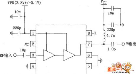
RF signals (RF) is input by pin 3 and output by pin 7 after enlarging by pre-amplifier and power amplifier. Pin 3 is directly coupled with internal amplifier. So, it adds a 10pF blocking coupling capacitor. The matching impedance is 50Ω when it works at 1880MHz. Pin 7 is output end of collector, whichcan connect power supply Vcc through choke or matching inductance. The typical matching impedance of this pin is 50Ω. In order to get the largest output power and efficiency, it connects to matching network outside to make the output impedance of amplifier match with it. Pin 1 is power down controlling end. The circuitworks when VPD=2.8V±0.1V (typical value of IPD is 8.5mA) and is closed when VPD<0.9V. VFD needs to add RF bypass circuit.
(View)
View full Circuit Diagram | Comments | Reading(741)
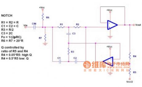
The circuit diagram of log amplifier
Published:2011/10/23 21:40:00 Author:May | Keyword: log amplifier

View full Circuit Diagram | Comments | Reading(1498)
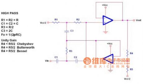
Third-order asymmetric filter circuit diagram composed of LM356 op amp
Published:2011/10/18 3:26:00 Author:Rebekka | Keyword: Third-order asymmetric filter, op amp
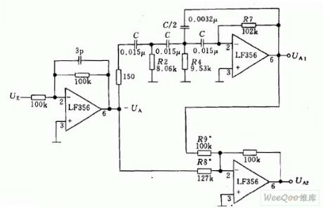
Filter circuit composed of third-order asymmetric composed of LM356 op amp is shown as above. Third-order filter has two outputs A1 and UA2. The former one is high-pass filter output, another one is low-pass filter output. (View)
View full Circuit Diagram | Comments | Reading(4160)
TDA2611AQ audio power amplifier IC circuit diagram
Published:2011/9/13 2:29:00 Author:Rebekka | Keyword: audio power amplifier , IC
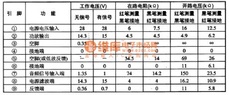
TDA2611AQ is an audio power amplifier integrated circuit produced by Philips of the Netherlands, It is widely used in video, audio, computer audio systems as audio power amplifier. The integrated circuit TDA2611AQ contains audio power amplifier IC circuits, overheating and output short-circuit protection circuit. The connected elements R, C between (5) and (9) feet can increase the input impedance. The IC uses separate 9-pin package, its integrated circuit pin functions and data are listed in Table. (View)
View full Circuit Diagram | Comments | Reading(1487)
Hi fi audio power amplifier circuit
Published:2011/8/24 2:26:00 Author:Jessie | Keyword: Hi fi audio power amplifier
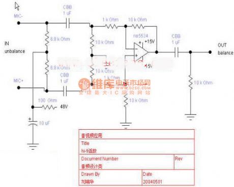
Hi fi audio power amplifier circuit: if you want to get high quality recording, you should have a good phone,but you must use high quality amplifier. This amplifier uses the tiny distortion ne5534, and itis listening to be soft and delicate. (View)
View full Circuit Diagram | Comments | Reading(1097)
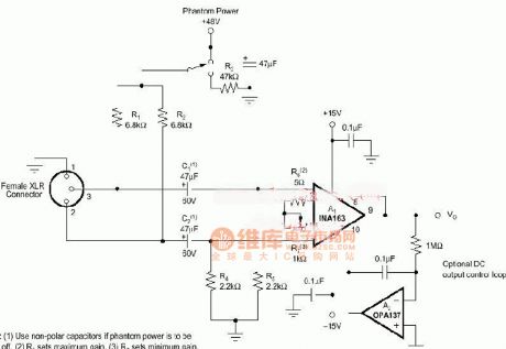
INA163 Microphone amplifier circuit diagram
Published:2011/8/24 2:24:00 Author:Jessie | Keyword: Microphone amplifier
View full Circuit Diagram | Comments | Reading(1730)
Double op-amp realization circuit diagram 3
Published:2011/8/19 1:05:00 Author:Jessie | Keyword: Double op-amp realization
View full Circuit Diagram | Comments | Reading(744)
Double op-amp realization circuit diagram 2
Published:2011/8/19 1:05:00 Author:Jessie | Keyword: Double op-amp realization
View full Circuit Diagram | Comments | Reading(695)
| Pages:54/250 At 204142434445464748495051525354555657585960Under 20 |
Circuit Categories
power supply circuit
Amplifier Circuit
Basic Circuit
LED and Light Circuit
Sensor Circuit
Signal Processing
Electrical Equipment Circuit
Control Circuit
Remote Control Circuit
A/D-D/A Converter Circuit
Audio Circuit
Measuring and Test Circuit
Communication Circuit
Computer-Related Circuit
555 Circuit
Automotive Circuit
Repairing Circuit