
Amplifier Circuit
Index 55
Double op-amp realization circuit diagram 1
Published:2011/8/19 1:04:00 Author:Jessie | Keyword: Double op-amp realization
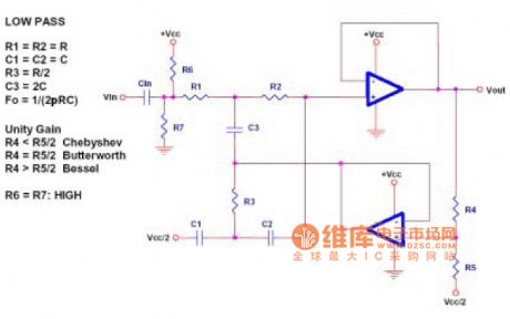
View full Circuit Diagram | Comments | Reading(830)
Single op-amp realization circuit diagram
Published:2011/8/19 2:04:00 Author:Jessie | Keyword: Single op-amp realization
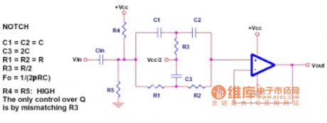
If it uses the band-pass filter composed of the components with parameters being very closed, it is prone to oscillation. The resistor connected to should be selected in E-96 1% series, or you will destroy the oscillation conditions. (View)
View full Circuit Diagram | Comments | Reading(762)
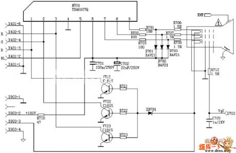
TDA6103 video amplifier circuit diagram
Published:2011/10/14 3:14:00 Author:Ecco | Keyword: video amplifier
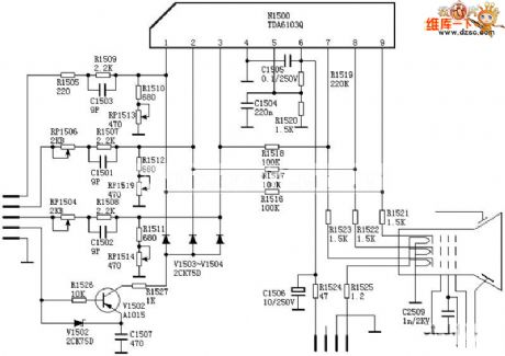
View full Circuit Diagram | Comments | Reading(3206)
The typical self-bias power amplifier stage circuit of tube
Published:2011/10/14 1:48:00 Author:Ecco | Keyword: self-bias , power amplifier , tube
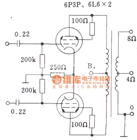
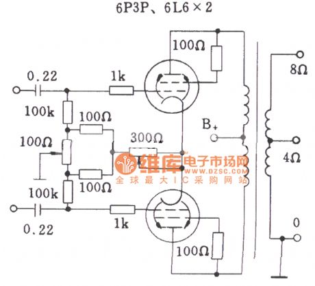
The typical self-bias power amplifier stage circuit withoutdebugging of tube
The typical semi-debugself-bias power amplifier stage circuit of tube
(View)
View full Circuit Diagram | Comments | Reading(1478)
TDA6107 video amplifier circuit diagram
Published:2011/10/14 2:11:00 Author:Ecco | Keyword: video amplifier
View full Circuit Diagram | Comments | Reading(8018)
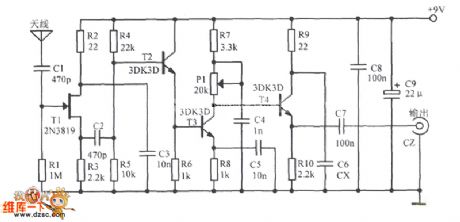
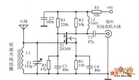
A short-wave signal amplifier circuit diagram
Published:2011/10/14 2:21:00 Author:Ecco | Keyword: short-wave signal amplifier
View full Circuit Diagram | Comments | Reading(1069)
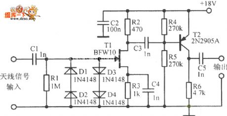
Broadband short-wave amplification circuit diagram
Published:2011/10/14 2:12:00 Author:Ecco | Keyword: Broadband short-wave amplification
View full Circuit Diagram | Comments | Reading(909)
Short-wave signal amplifier circuit diagram
Published:2011/10/14 2:13:00 Author:Ecco | Keyword: Short-wave signal amplifier
View full Circuit Diagram | Comments | Reading(1474)
Low-noise amplifier circuit diagram
Published:2011/10/16 22:33:00 Author:Ecco | Keyword: Low-noise amplifier
View full Circuit Diagram | Comments | Reading(2405)
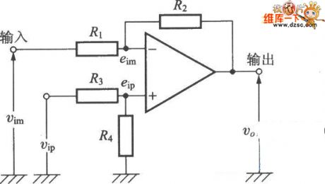
Differential amplifier circuit diagram
Published:2011/10/17 1:13:00 Author:Ecco | Keyword: Differential amplifier
View full Circuit Diagram | Comments | Reading(948)
Common TDA6108 video amplifier circuit
Published:2011/10/14 3:12:00 Author:Ecco | Keyword: Common video amplifier
View full Circuit Diagram | Comments | Reading(4888)
TDA5112 video amplifier circuit diagram
Published:2011/10/14 2:24:00 Author:Ecco | Keyword: video amplifier
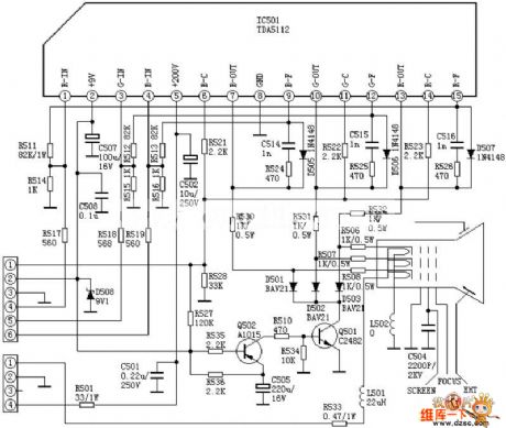
View full Circuit Diagram | Comments | Reading(2081)
JFET gate grounding preamplifier circuit diagram
Published:2011/9/15 1:38:00 Author:Rebekka | Keyword: JFET gate grounding preamplifier
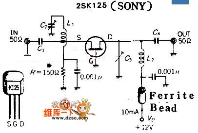
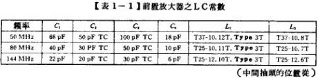
Figure 1-1 is the example of joint types FET 2SK125(SONY) grounded gate amplifier. So when you use the gate grounding circuit, you could separate the input and output by using the grounding gate electrode on printing copper foil. The power gain of the circuit is about 10~12dB, NF is about 2dB. The LC value in the circuit change with frequency. You should choose table 1-1, and L1, L2 are at toroidal core amine line of poly resin. The diameter is about 0.3mm. It should insert in the substrate directly to avoid producing stray capacitance. You could Adding a source of resistor where you want to adjust and keep the drain current being about 10mA. In addition, adjusting trimmer condenser can get the highest sensitivity. (View)
View full Circuit Diagram | Comments | Reading(3452)
1M ~ 50MHZ 1W broadband power amplifier circuit diagram
Published:2011/9/15 1:35:00 Author:Rebekka | Keyword: broadband power amplifier
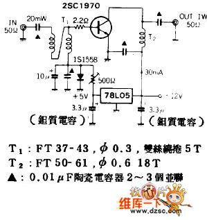
The picture shows the 1W wide-broadband power amplifier with frequency in 1 ~ 50MHz and using 2SC1970; Input and output coils use broadband transformer composed of toroidal winding for impedance conversion. 2SC1970 is the 170MHz power transistor, so it can be used for the VHF band broadband amplifier. In the circuit , the coupling capacitor (CoupIingCapacitor) and Bypass Capacitor are connected with 2 to 3 0.01μF ceramic capacitor in parallel, the most important thingis to reduce the impedance (Impedance), at the same time, the current flows the channel is also wider. (View)
View full Circuit Diagram | Comments | Reading(2964)
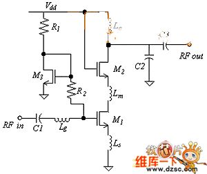
10M-1200MHZ and μPC1651G broadband amplifier circuit diagram
Published:2011/9/14 21:41:00 Author:Rebekka | Keyword: broadband amplifier circuit
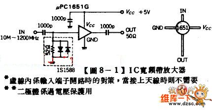
μPC1651G(Japanese electrical apparatus) series use high-frequency broadband amplifier. Micro-disc shape(Micro Disk Type). Frequency coverage is 10M~1200MHz(@-3dB), and the gain is 19dB(@f=500MHz). NF is about 5dB, so it's not good to use receiver preamplifier. But there is not much effect on using receiver preamplifier and IF amplifying circuit. Figure 1 is broadband preamplifier composed of μPC1651G. Although it has a simple structure, you should pay attention to the effect of lead inductance when youwant to get1200MHz, so it is better to use short wiring. The circuit cases use broadband amplifier composed of glass epoxy double-sided substrate. The bypass capasitor of power terminal should be connected between IC power supply and ground. It should be near to IC.
(View)
View full Circuit Diagram | Comments | Reading(1653)
Operational amplifier general zero setting method circuit diagram
Published:2011/9/26 21:21:00 Author:Rebekka | Keyword: Operational amplifier , zero setting method
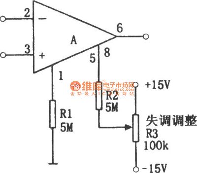
The figure shows a simple common zero seting circuit. Its integrated chip can be used for the OPA37, LH0044B and so on. As the adjustment of the network (R1, R2 and R3 form a potentiometer) uses the 15V positive and negative power supply, almost any amplifier is suitablefor zero seting. ①, ⑧ pins are zero ends. The resistors R1 and R2 are high-value resistors. It is usually taken to be 5MΩ for the LH0044B. It only has a few microamps of current and plus an adjustable voltage on R2, so that the two currents are imbalance and adjust the offset voltage. (View)
View full Circuit Diagram | Comments | Reading(891)
Microphone amplifier circuit diagram
Published:2011/8/3 2:33:00 Author:Ecco | Keyword: Microphone amplifier
View full Circuit Diagram | Comments | Reading(930)
In-phase composite DC amplifier circuit diagram
Published:2011/9/19 1:16:00 Author:Ecco | Keyword: In-phase , composite DC amplifier
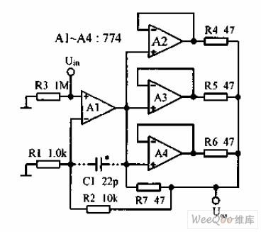
It uses the four operational amplifier 774 to achieve its parallel work, andit can drive 500Ω loads with goodlinear in the ± 10V range.
(View)
View full Circuit Diagram | Comments | Reading(1012)
Power amplifier circuit of Marantz electronic valve 8
Published:2011/9/25 22:11:00 Author:Ecco | Keyword: Power amplifier , Marantz, electronic valve
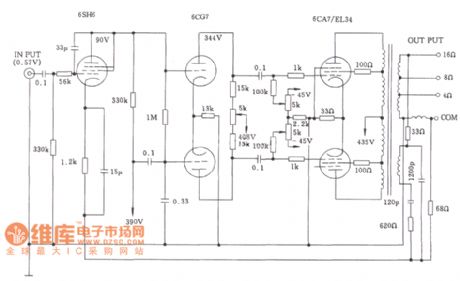
Whole frequency response rangeis relatively flat from 10Hz to 40Hz.
(View)
View full Circuit Diagram | Comments | Reading(1559)
Tube SRPP inverter circuit
Published:2011/9/25 22:17:00 Author:Ecco | Keyword: Tube SRPP inverter
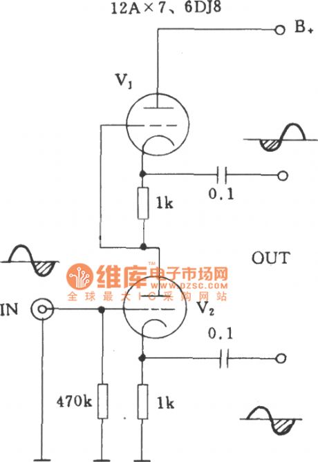
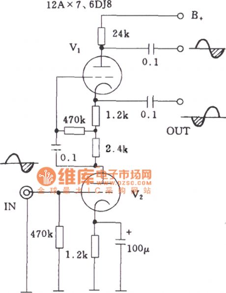
SRPP tube common-cathode inverter circuit:
Tube SRPP common-gateinvertercircuit:
(View)
View full Circuit Diagram | Comments | Reading(2680)
| Pages:55/250 At 204142434445464748495051525354555657585960Under 20 |
Circuit Categories
power supply circuit
Amplifier Circuit
Basic Circuit
LED and Light Circuit
Sensor Circuit
Signal Processing
Electrical Equipment Circuit
Control Circuit
Remote Control Circuit
A/D-D/A Converter Circuit
Audio Circuit
Measuring and Test Circuit
Communication Circuit
Computer-Related Circuit
555 Circuit
Automotive Circuit
Repairing Circuit