
Amplifier Circuit
Index 48
Current feedback amplifier circuit of broadband transconductance operational amplifier and buffer OPA660
Published:2012/8/13 22:03:00 Author:Ecco | Keyword: Current feedback , amplifier, broadband , transconductance, operational amplifier , buffer
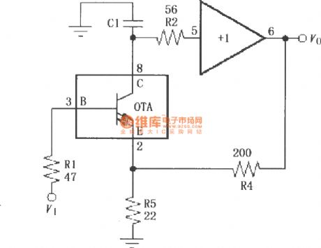
Signal V1 is input to pin 3 of OPA660 by 47Ω resistor and output from pin 6 after being amplified by the internal +1 amplifier; at the same time, pin 2 of OPA660 gets feedback from pin 6 by 200Ω resistor to constitute the current feedback amplifier. The current feedback amplifier can be used to stabilize static operating point, expand broadband and reduce the output distortion of amplifier. Circuit gain G = 1 + R4/R5 = 10.
(View)
View full Circuit Diagram | Comments | Reading(1574)
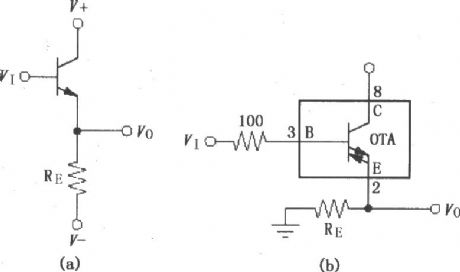
Common emitter (common -E) amplifier circuit of broadband transconductance operational amplifier and buffer OPA660
Published:2012/8/13 22:09:00 Author:Ecco | Keyword: Common emitter , common -E, amplifier , broadband , transconductance, operational amplifier , buffer
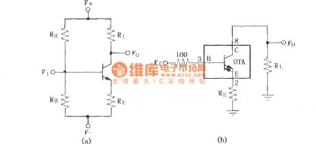
Figure (a) shows the discrete componentscommon- emitter amplifier, andtransconductance changes in the whole temperature range , Vo is the inverting gain , Vos only has a few volts. Figure (b) shows common emitter amplifier composed of the OPA660, andthe transconductance is a constant in the whole temperature range, Vo is the in-phase gain , Vos = 0V.
(View)
View full Circuit Diagram | Comments | Reading(768)
Digital 440MBit / s sending system driver amplifier circuit composed of OPA2662
Published:2012/8/13 21:53:00 Author:Ecco | Keyword: Digital , 440MBit / s , sending system , driver , amplifier
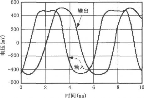
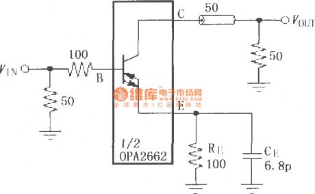
Input and output impulse response waveforms are shown as below. The cicuit uses an OTA which is inside of OPA2662 to constitute a common-emitter amplifier, that is, the input -end is added 100Ω current limiting resistor and 50Ω matching resistor, then the signal is amplified and output to drive 50Ω cable and load. Io = ± 17mA.
(View)
View full Circuit Diagram | Comments | Reading(775)
Common collector (common -C) amplifier circuit of broadband transconductance operational amplifier and buffer OPA660
Published:2012/8/13 22:11:00 Author:Ecco | Keyword: Common collector , common -C, amplifier , broadband , transconductance , operational amplifier, buffer
G=1. Figure (a) shows the discrete components common-collector amplifier , Vos = 0.7V ; Figure ( b ) shows common-collector amplifier ( buffer ) composed of OPA660, Vos, = 0V.
(View)
View full Circuit Diagram | Comments | Reading(1272)
The caple amplifier circuit composed of OPA660
Published:2012/8/12 22:10:00 Author:Ecco | Keyword: caple amplifier
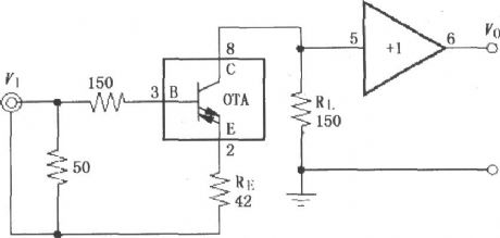
Cable input signal VI is added to the pin 3 of OPA660 after passing 150Ω base resistor and 50Ω matched resistor, then it is output by pin 6 after being amplified by the internal OTA and +1 amplifier ( resistor RQ is not shown in figure in quiescent current ). Circuit gain G = RL / (RE + rE ) = +3.
(View)
View full Circuit Diagram | Comments | Reading(1146)
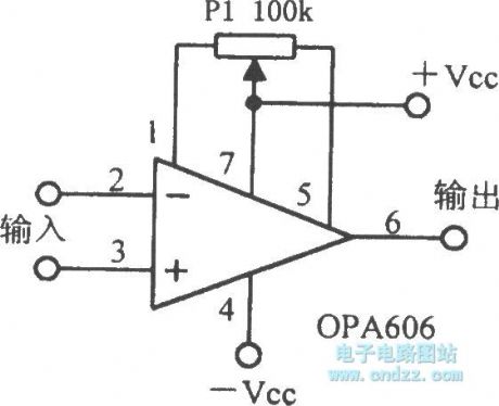
The OPA606 broadband Difet operational amplifier circuit
Published:2012/8/11 1:43:00 Author:Ecco | Keyword: broadband , Difet, operational amplifier
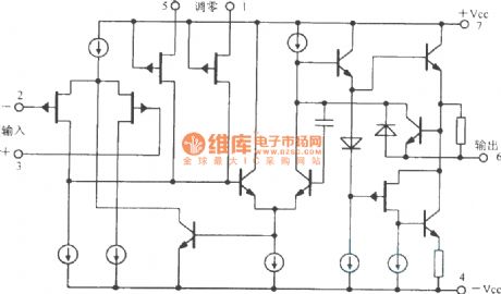
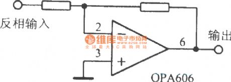
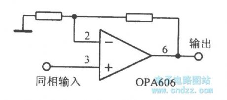
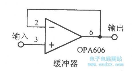
Simplified schematic:
The zeroing cable diagram:
noninverting amplifier:
inverting amplifier:
Buffer wiring diagram:
(View)
View full Circuit Diagram | Comments | Reading(1259)
Current-comparator NORTON four op amp MC3301/3401
Published:2012/8/6 4:29:00 Author:Ecco | Keyword: Current-comparator, NORTON, four op amp
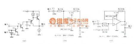
Figure (a)is simplifiedschematic diagram; Figure(b)is the inverting input amplifier circuit; Figure (c)is the noninverting input amplifier circuit.
(View)
View full Circuit Diagram | Comments | Reading(1516)
The basic op amp circuit for voltage stabilization
Published:2012/8/6 4:35:00 Author:Ecco | Keyword: basic op amp , voltage stabilization
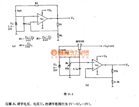
In the circuir, the value of R1~R3 can be selected by the required regulated value. UA is higher than UZ. The voltageof circuit shown in the figure b can be regulated by RP. The regulating range of voltage UA is about 2V~(UB-2V).
(View)
View full Circuit Diagram | Comments | Reading(1201)
Voltage-controlled 4W audio amplifier circuit diagram
Published:2012/7/11 2:14:00 Author:Ecco | Keyword: Voltage-controlled , 4W , audio amplifier
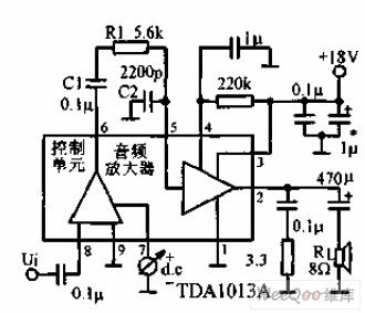
Voltage-controlled 4W audio amplifier uses audio amplification IC TDA103Ato provide4W of output power. The control voltage is3.5 ~ 8V, and controlcharacteristic is logarithmic with controlling rangein 80dB.
(View)
View full Circuit Diagram | Comments | Reading(1593)
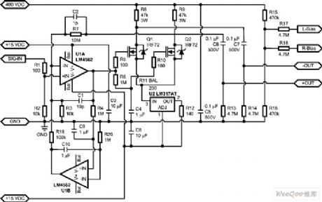
100W amplifier circuit diagram with DC 500KHZ
Published:2012/7/11 2:19:00 Author:Ecco | Keyword: 100W , amplifier , DC 500KHZ
The 100W amplifier with DC 500KHzuses the features of high input impedance , high gainofa photoelectric op amp to make output power be 100W. Load current can be up to 10A, and it requires high current wiring and capacitance power supply bypass . This circuit is used for high - fidelity audio circuits, cathode-ray deflection and servo system.
(View)
View full Circuit Diagram | Comments | Reading(2229)
ESL amplifier circuit diagram
Published:2012/7/11 2:11:00 Author:Ecco | Keyword: ESL amplifier
When the design shown in the figure is connected to the popular Stax 1 electrostatic headphones, it can transmit 200Vp - p voltage on full audio bandwidth. Although you can change the resistor divider to provide a bias voltage of up to 400VDC, the device shown in figure uses DC 200V bias. As many kinds of Stax headphones have similar driver and bias demands, the design also applies to these models.
(View)
View full Circuit Diagram | Comments | Reading(2369)
The amplifier circuit diagram composed of M5106P
Published:2012/7/3 22:06:00 Author:Ecco | Keyword: amplifier
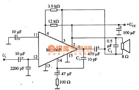
Figure 4-42 shows the amplifier circuit composed of M5106P. The circuit can be used as main power amplifier with output power in 1W. As the M5106P has no zero end, it is very easy to use. In order to make the circuit operation stably, you should note the following : pin 13 and pin 15 are grounded to the input end, and pin 1 and pin 14 should access phase compensation capacitor C1 to prevent the oscillating capacitance from connecting 8Ω speaker load. When the supply voltage is 9V , the output power is 1W; when the power supply voltage is 6V, it only can receive 0.5W output.
(View)
View full Circuit Diagram | Comments | Reading(2278)
High precision selective amplifier circuit diagram
Published:2011/7/28 1:24:00 Author:Nicole | Keyword: High precision, selective amplifier
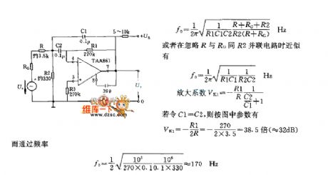
The ordinary selective amplifier adopts double T network, it requires thatthe component parameters have high precision. But if you use the circuit as shown in the figure, you can avoid it. At the low pass, the passing frequency f0 is determined by C1, and by C2 at the high pass.
(View)
View full Circuit Diagram | Comments | Reading(1643)
Preamplifier circuit of 1m laser metroscope fringe counter
Published:2011/12/1 20:25:00 Author:May | Keyword: Preamplifier, 1m laser metroscope, fringe counter
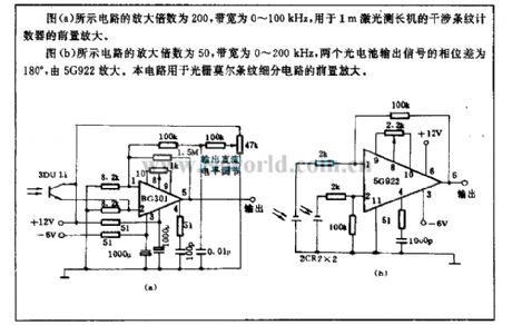
The amplification factor of the circuit shown in diagram (a) isis 200, and itsbandwidth is 0~100kHz. And it isused forpreamplification of 1m laser metroscope interference fringe counter.
The circuit shown in diagram (b) is used for preamplication of grating moire fringe subdivision circuit. Its magnification times is 50. Its bandwidth is 0~200kHz. Phase separation of two electric eye outcoming signal is 180° and is amplified by 5G922.
(View)
View full Circuit Diagram | Comments | Reading(1419)
Precision photoelectric detection isolated amplifier ( ISO212 ) circuit
Published:2011/8/31 1:50:00 Author:Jessie | Keyword: photoelectric detection , isolated amplifier
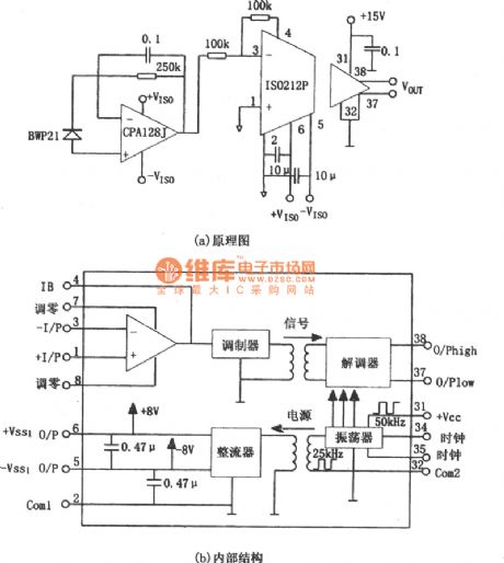
The circuit adopts jfetinput integrated amp OPA128. This amp has very low offset current, which is about 40~150fA (1fA=10-15A),so its input impedance is extremely high (is about 1013//lΩ//pF), it andphotoelectric diode BPW21 form the photoelectric detection circuit with excellent performance. The photoelectric detection circuit will change light signals into electrical signals, andit issent to photoelectric coupling isolated amplifier ISO212P after amplifing,and that is the photoelectric detection isolated amplifier. (View)
View full Circuit Diagram | Comments | Reading(2219)
The voltage-dividing bias amplifier circuit diagram of mosfet
Published:2011/8/24 2:21:00 Author:Jessie | Keyword: voltage-dividing bias amplifier, mosfet
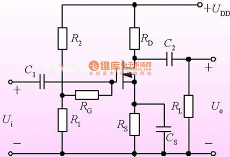
View full Circuit Diagram | Comments | Reading(1211)
Common emitter amplifying circuit
Published:2011/8/24 2:19:00 Author:Jessie | Keyword: Common emitter, amplifying
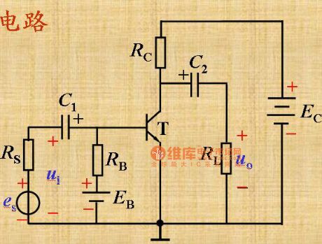
Common emitter amplifying circuit
The amplifier's role: amplifiering faint signals (voltage, current, and power) to the required category. The role of each element: Transistor T-- The amplification component, iC = b iB. It must ensure the collector junction reverse bias, the emitter biased to make the transistor work in the enlarged area. Base power EB and base resistor RB-- Make emitterforward bias, and provide the proper size base current. Collector power EC-- Provide the energy for the circuit. And guarantee BC junction reverse bias. The collector resistance RC-- Change current amplification to voltage amplification. Coupling capacitors C1, C2--theyisolate input, output and amplifying circuit DC's link to beAC signal input and output smoothly. (View)
View full Circuit Diagram | Comments | Reading(1284)
Differential input/output gain programmable amplifier circuit
Published:2011/8/30 21:23:00 Author:Jessie | Keyword: Differential input/output, gain programmable, amplifier
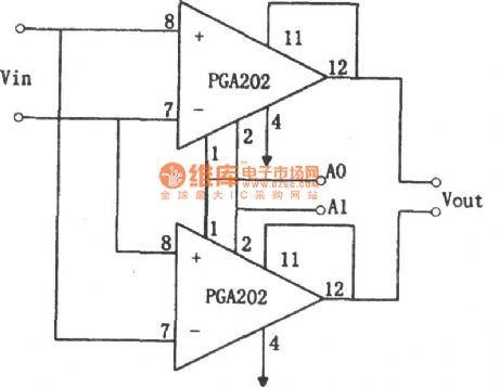
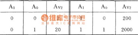
As shown in the chart, the circuitis thedifferential input/output gain programmable amplifier circuit. This circuit is composedof two pieces of PGA202 integrated circuits. PGA202 is mosfet input instrument integrated amp, and its gain has four different values: 1, 10, 100 and 1000. In circuit A0 (pin 1) and A1 (pins 2)are gain control terminals. when A0 and A1 are at different levels ( 1 or 0 ),their gainvalues aredifferent. Because here is two amplifier circuits using parallel form, thus circuits' total gain is twice of the monolithic gain , namely Vo = 2Av1Vi. Av1 ismonolithic amplifier circuit's gain, so the circuit's total gain is Av2 = 2Av1. CorrespondingAv2's valuesalso have four: 2, 20, 200, 2000. The relationship betweenthe total gain Av2 and gain control ports A0, A1 is listed in table. (View)
View full Circuit Diagram | Comments | Reading(1011)
Used for floating-point transform gain variable buffer amplifier circuit
Published:2011/8/31 1:14:00 Author:Jessie | Keyword: floating-point transform, gain variable, buffer amplifier
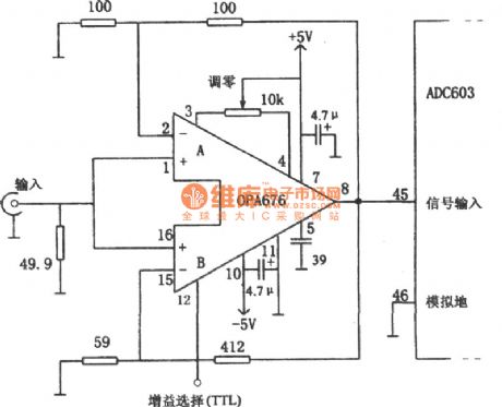
As shown in figure, the circuitis floating-point transform gain variable buffer amplifier circuit. The circuit consists of two parts: the buffer amplifier composedof OPA676 and theA/D conversion interface circuitcomposedof ADC603. OPA676 integrated chip's internal has two characteristics identical but independent differential amplification input levels. The two channels A and B can realize strobe by choosing pin 12's level. That is, when pins 12 is ata high level, channel A works, channel B cuts off; When pin 12 isat a low level, channel A cuts off, channel B works. The two channels' gains are different, using pin 12'scorresponding chose can realize gain's choice. We can learn from the diagram: Channel A voltage magnification is AVA=1+R2/R1=2; Channel B's voltage magnification is AvB=1+R4/R3=1+412/59=8. (View)
View full Circuit Diagram | Comments | Reading(1047)
400MHz differential amplifiering circuit
Published:2011/8/30 2:49:00 Author:Jessie | Keyword: differential amplifier
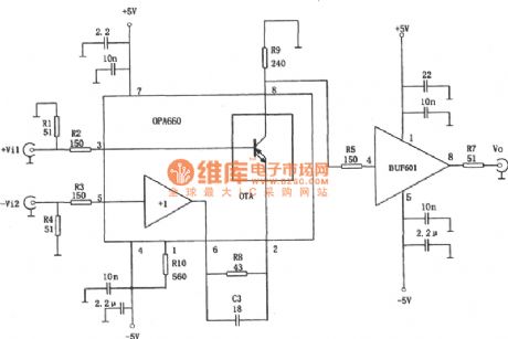
As shown in figure, the circuitis 400MHz broadband differential amplifying circuit. This circuit consists of two parts: the input broadband differential amplifier of integrated chip OPA660 and the caching amplifying circuit composedof BUF601. This circuit's voltage magnification is: Av=R9/(R8+1/gm), gm is the transconductance OPA660's transconductance amplifier OTA. Because in the chart the resistance R10=560Ω, OPA660's static current is about 10mA, at this timethe transconductance is gm=82mA/V. (View)
View full Circuit Diagram | Comments | Reading(823)
| Pages:48/250 At 204142434445464748495051525354555657585960Under 20 |
Circuit Categories
power supply circuit
Amplifier Circuit
Basic Circuit
LED and Light Circuit
Sensor Circuit
Signal Processing
Electrical Equipment Circuit
Control Circuit
Remote Control Circuit
A/D-D/A Converter Circuit
Audio Circuit
Measuring and Test Circuit
Communication Circuit
Computer-Related Circuit
555 Circuit
Automotive Circuit
Repairing Circuit