
Amplifier Circuit
Index 47
GaAsFET amplifier circuit
Published:2012/9/10 21:02:00 Author:Ecco | Keyword: GaAsFET amplifier
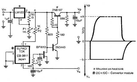
The control circuit operates to double from a positive supply, which, when turned on the power of the first door. and goes off when the first drain as shown in FIG. This circuit integrates the LM123, a three-terminal positive regulator and a dc dc + converter, whose output power drains and gates of GaAsFET-power relay in a power amplifier. The controller output drives a three-terminal DC + DC converter - which exit through an N-channel lFET properly so as to pull the base of the series pass transistor 2N6107 at a level to turn it on.
Source: discovercircuits (View)
View full Circuit Diagram | Comments | Reading(802)
Programmable gain amplifier
Published:2012/9/10 21:02:00 Author:Ecco | Keyword: Programmable gain , amplifier
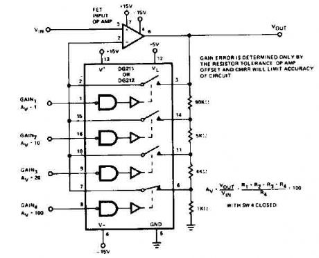
The circuit uses the DG212 which controlling the gain using resistors. To calculate the different gains SW4 should be closed. Gain error is determined only by the resistor tolerance op amp offset and CMR will limit accuracy of circuit.
Source: discovercircuits (View)
View full Circuit Diagram | Comments | Reading(0)
Offset controlled stereo amplifier circuit
Published:2012/9/10 21:02:00 Author:Ecco | Keyword: Offset controlled, stereo amplifier
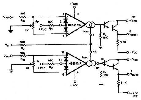
This stereo amplifier use the NE5517/A and has an excellent tracking of 0.3 dB typical easy. With the potentiometer, Rp, the offset can be adjusted. For AC-coupled amplifiers, the knob can be replaced by two resistors 5.1 k ohm.
Source: discovercircuits (View)
View full Circuit Diagram | Comments | Reading(2)
Unity gain Inverter amplifier circuit
Published:2012/9/10 21:01:00 Author:Ecco | Keyword: Unity gain , Inverter, amplifier
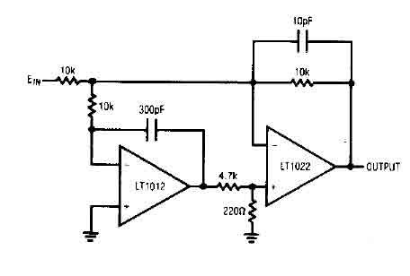
The circuit consists of a device with low drift LTl012. and a speed amplifier LTl022Jligh. The entire circuit is a unity gain inverter, with the summing node at the junction of three resistors 10k. The monitors what the Tl012 summing node, it compares to the mass, and drives the positive input LTI022, completing a loop to stabilize around the Tl022 L. The k 10 to 300 pF at the time constant LTI012 limit its response to low frequency signals. LTl022 handles the high-frequency inputs while LTl012 stabilizes the operating point.
Source: discovercircuits (View)
View full Circuit Diagram | Comments | Reading(1386)
Simple logarithmic amplifier circuit
Published:2012/9/10 21:01:00 Author:Ecco | Keyword: Simple , logarithmic, amplifier
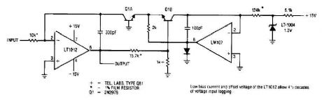
This simple logarithmic amplifier circuit use the LT1012 which has a low bias current allow 4 1/2 decades off voltage input logging.
Source: discovercircuits (View)
View full Circuit Diagram | Comments | Reading(2866)
High gain amplifier circuit
Published:2012/9/10 21:01:00 Author:Ecco | Keyword: High gain , amplifier
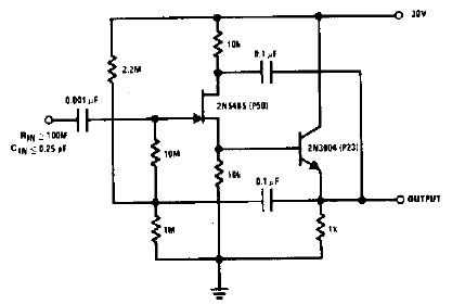
In this circuit nothing is left to chance in reducing input capacitance. The 2N5485, which has a very low-capacity legacy first, is always operated as a source follower with gate bias bootstrap.
Source: discovercircuits (View)
View full Circuit Diagram | Comments | Reading(2638)
2 Watt stereo amplifier with LM1877N-9
Published:2012/9/10 20:59:00 Author:Ecco | Keyword: 2 Watt , stereo amplifier
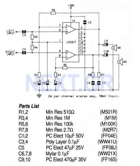
This circuit uses a stereo amplifier IC in a 14-pin DIL package that requires very few external components to make a complete 2 Watt per channel power amplifier.
Source: discovercircuits (View)
View full Circuit Diagram | Comments | Reading(1)
Stereo Preamplifier with balance and loudness
Published:2012/9/10 20:58:00 Author:Ecco | Keyword: Stereo Preamplifier , balance , loudness
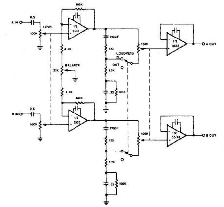
The circuit of preamplifier use the 5533 chip and features a combination of controls balance and volume. Due to the nonlinearity of the human auditory system, low frequencies must be boosted at low listening levels. Level pay, and LOUDNESS controls provide all the plays to produce the desired response from the music.
Source: discovercircuits (View)
View full Circuit Diagram | Comments | Reading(5078)
Amplifier Compressor MC3340P
Published:2012/9/10 20:54:00 Author:Ecco | Keyword: Amplifier , Compressor
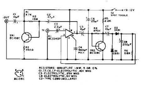
This audio compressor circuit use a MC3340P as a variable gain amplifier. The output is rectified and TR2 controls the gain of the ICL ..
Source: discovercircuits (View)
View full Circuit Diagram | Comments | Reading(3608)
AUDIO AMP + 3KHz FILTER
Published:2012/9/6 20:48:00 Author:Ecco | Keyword: AUDIO AMP, + 3KHz, FILTER

This circuit is the audio amp section for a complete optical transmitter. The circuit amplifies and filters the voice audio signals from an electret microphone. The circuit is described in more detail in the receiver section of Dave Johnson's Handbook of Optical Through the Air Communications.
Source: discovercircuits (View)
View full Circuit Diagram | Comments | Reading(2591)
40KHz Limiting Amp
Published:2012/9/6 20:46:00 Author:Ecco | Keyword: 40KHz, Limiting Amp
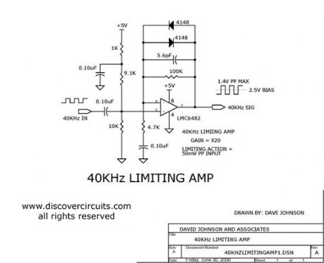
This circuit has a gain of X20 at 40KHz. The amplifier output level is limited to 2.5v peak to peak. Limiting action begins with a 50v peak to peak input.
Source: discovercircuits (View)
View full Circuit Diagram | Comments | Reading(2054)
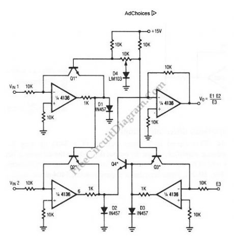
Analog Multiplier-Divider with 4136 Op-Amps
Published:2012/9/3 1:39:00 Author:Ecco | Keyword: Analog Multiplier-Divider, Op-Amps
Source: freecircuitdiagram
This unique circuit below can be used as divider and multiplier. This circuit is formed by all four sections of a 4136 . The Q1 through Q4 can be any PNP transistor, but that must matched transistors. The transistor matching determine the acurracy of the divider and multiplier circuit. Here is the schematic diagram of the circuit:
(View)
View full Circuit Diagram | Comments | Reading(4232)
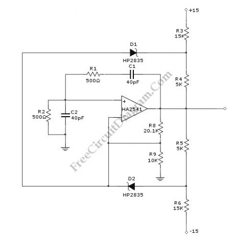
Wien-Bridge Oscillator Using HA2541 Op-Amp
Published:2012/9/3 1:38:00 Author:Ecco | Keyword: Wien-Bridge, Oscillator , Op-Amp
Source: freecircuitdiagram
A Wien-Bridge oscillator circuit can be built from HA2541 and some basic components. This circuit can generate good-quality sine wave of 40 MHz with an upper limit of 50 MHz. The R3 through R7 and D2 and D1 provide the diode limiting for this circuit. Here is the schematic diagram of this circuit:
(View)
View full Circuit Diagram | Comments | Reading(1313)
Common-emitter amplifier circuit composed of double broadband transconductance operational amplifier OPA2662
Published:2012/8/28 2:44:00 Author:Ecco | Keyword: Common-emitter amplifier, double broadband , transconductance , operational amplifier
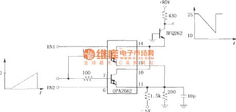
The circuit uses the OPA2662 internal dual OTA connected in parallel to constitute a common-emitter amplifier. The input end is connected 100Ω current limiting resistor in parallel, the input signal is input by 2 feet and 7 feet. 14 feet and 10 feet are connected the collector, 15 feet and 11 feet are connected to constitute the emitter, BFQ262 and 430Ω resistor form collector load, and the signal will be output after beng amplified, and the input and output waveforma are shown in Fig.
(View)
View full Circuit Diagram | Comments | Reading(838)
+12V single supply sampling instrument amplifier circuit with protective driver composed of SMP04 and instrument amplifier
Published:2012/8/28 2:39:00 Author:Ecco | Keyword: +12V, single supply , sampling instrument , amplifier , protective driver , instrument amplifier
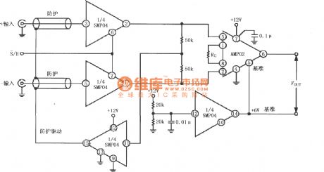
The circuit also uses the two channels of sample and hold amplifier SMP04 to constitute differential sampling with instrumentation amplifier AMP02. The signal is input (±) to SMP04, then it is differential amplified and output after being sampling and holding by AMP02. The other two sample-and-hold amplifiers' control terminal S / H are always grounded to keep the sample state. One is used to drive shielded cable to protect it from the interference from common-mode voltage; the other one is used to provide +6 V reference voltage for AMP02.
(View)
View full Circuit Diagram | Comments | Reading(1573)
AD585 high-speed precision sampling and maintaining amplifier
Published:2012/8/23 22:15:00 Author:Ecco | Keyword: high-speed, precision , sampling , maintaining, amplifier
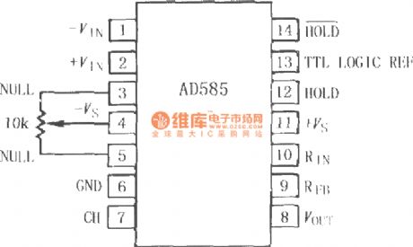
The AD585 is a complete monolithicsampling and maintaining amplifier, including a high-performance operational amplifier series with a very low leakage current switch and a FET input integrated amplifier. The internal holding capacitor and matching applications resistors provide precision and flexibility. The AD585's quick sampling time, low sample-and-hold disorders and fall characteristics make it ideal for high-speed 10 ~ 12bit data acquisition system. The pin configuration is shown as the figure.
(View)
View full Circuit Diagram | Comments | Reading(919)
4127 logarithmic amplifier
Published:2012/8/22 20:44:00 Author:Ecco | Keyword: logarithmic amplifier
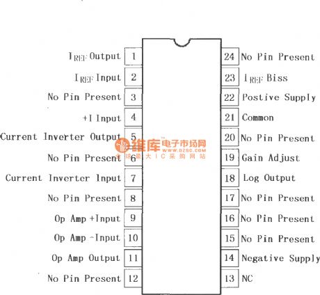
4127 is the first hybrid logarithmic amplifier with double width DIP ceramic package, it can accept either polarity signal from the current source or voltage source. 4127 is the ASIC chip for logarithmic transformation with accurate 6 decimal input current and 4 decimal input voltage. In addition, a current inverter and an internal precision reference make pin programmable to complete the functions of logarithmic, logarithmic ratio and antilog amplifier. In order to further increase its versatility and reduce the cost of the user's system, the internal 4127 encapsulates an operational amplifier which can be used as a buffer, filter or gain elements. The initial accuracy of 4127 is 0.5% and 1.0%, and it can work in ambient temperature range of -10 ~ +70 ℃. The 4127 versatility and high performance have many uses, such as signal compression, sensor linearization, light electrical buffer, as well as in the manufacturing of medical devices, analytical instrumentation and process control instruments.
(View)
View full Circuit Diagram | Comments | Reading(2396)
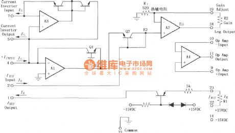
Precision logarithmic and logarithmic ratio amplifier LOG100
Published:2012/8/21 22:57:00 Author:Ecco | Keyword: Precision logarithmic , logarithmic ratio , amplifier
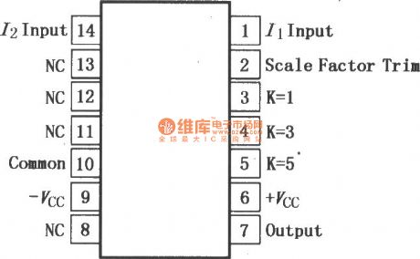
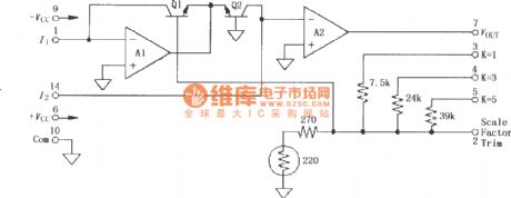
LOG100 uses advanced integrated circuit technology to achieve its high accuracy, and it is easy to use with low cost and small size to make logical logarithmic arithmetic. The maximum error of amplifier in specifications ensure is more than 6 decimal input range (1nA ~ 1mA) and all possible I1 and I2 combinations. As to ensure the total error, it does not require the calculation of the concerned error. The circuit uses a special design which is compatible with film monolithic integrated circuit, including amplifiers, logarithmic transistors and low drift thin-film resistors. In order to guarantee maximum precision, the thin film resistor uses laser correction.
(View)
View full Circuit Diagram | Comments | Reading(973)
Power line carrier amplifier circuit
Published:2012/8/21 1:15:00 Author:Ecco | Keyword: Power line carrier , amplifier
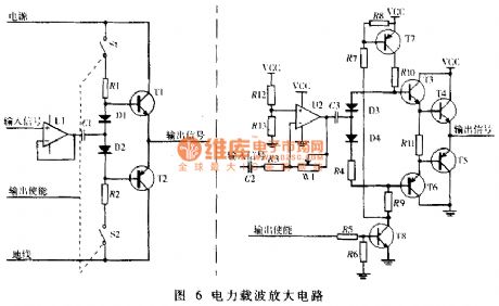
View full Circuit Diagram | Comments | Reading(2869)
Common base (common -B) amplifier circuit of broadband transconductance operational amplifier and buffer OPA660
Published:2012/8/13 22:06:00 Author:Ecco | Keyword: Common base, common -B, amplifier , broadband , transconductance , operational amplifier, buffer
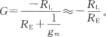
Figure (a) shows the discrete components common-base amplifier , Vo is the in-phase gain, Vos has a few volts; figure ( b ) shows the common-base amplifier composed of OPA660. Vo is the inverting gain , Vos = 0V.
(View)
View full Circuit Diagram | Comments | Reading(1390)
| Pages:47/250 At 204142434445464748495051525354555657585960Under 20 |
Circuit Categories
power supply circuit
Amplifier Circuit
Basic Circuit
LED and Light Circuit
Sensor Circuit
Signal Processing
Electrical Equipment Circuit
Control Circuit
Remote Control Circuit
A/D-D/A Converter Circuit
Audio Circuit
Measuring and Test Circuit
Communication Circuit
Computer-Related Circuit
555 Circuit
Automotive Circuit
Repairing Circuit