
Amplifier Circuit
Index 69
LINEAR_OUTPUT_RAMP
Published:2009/7/14 20:42:00 Author:May
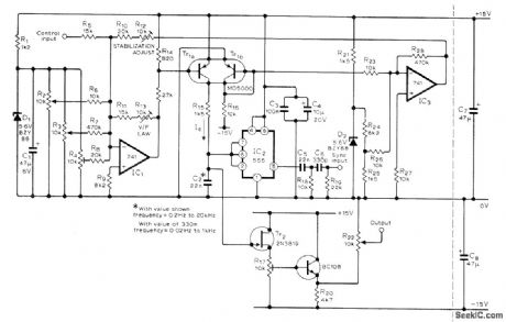
Provides high frequency stability as required for use in sound synthesizers. Can be synchronized to another oscillator. Uses 555 timer in astable mode, with Tr1a supplying constant current to C2. R12 and R13 should be multiturn pots. Synchronizing square-wave signal having 5-10 V peak can be fed in at R19 for differentiation, and resulting spikes used to control threshold voltage of 555. R4 sets minimum frequency. R22 sets average Output level to 0 V R2 and R3 serve as coarse and fine frequency controls Tr1 can also be BFX11 or BFX36. –T. W. Stride, Voltage Controlled Oscillator Wireless World, Oct . 1977, p 66.
(View)
View full Circuit Diagram | Comments | Reading(1374)
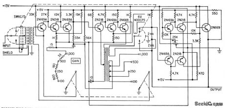
60_DB_LOW_NOISE_FET_AMPLIFIER
Published:2009/7/14 22:52:00 Author:Jessie
Gives maximum voltage gain of 60 db, constant within 0.5 db from -55 to +125℃ with built-in gain adjustment. Has good low-frequency response, along with extremely low noise, as little as 5 db at 10 cps. Used with low-level transducers, null detectors, recorders, oscilloscopes, and medical research equipment.-Texas Instruments Inc., Solid-State Communications, McGraw-Hill, N.Y., 1966, p 293. (View)
View full Circuit Diagram | Comments | Reading(984)
HLTRAHIGH_IMPEDANCE_AMPLIFIER
Published:2009/7/14 20:36:00 Author:May
Bridge balanced series-compensated d-c amplifier using ordinary vacuum tubes gives input impedance of 250,000 meg. For precise voltage measurements without loading high-impedance circuits,-J. Morrison. For precise Measurements An Ultrahigh Impedance Amplifier. Electronics.35:40,p49 (View)
View full Circuit Diagram | Comments | Reading(815)
FET_OPERATIONAL_AMPLIFIER
Published:2009/7/14 20:35:00 Author:May


Open-loop voltage gain at direct current is above 100,000. When operated open-loop, makes excellent voltage comparator having high resolution.-L. J. Sevin, Jr. Field-Effect Transistors, McGraw-Hill, N.Y. 1965, p107. (View)
View full Circuit Diagram | Comments | Reading(1385)
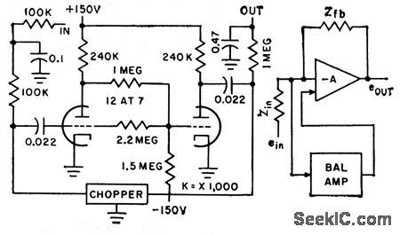
CHOPPER_TYPE_DATA_AMPLIFIER
Published:2009/7/14 20:33:00 Author:May
Careful design of transistor circuits between chopper input and chopper output gives gain stability within 0.01% for long-term operation (1,000 hours) front 15 to 35 C, linearity is equally precise for normal output range of plus or minus 10V.-F. Offner, Transistorized Data Amplifier Has High Gain-Stability, Electronics, 33:27, p 55-57. (View)
View full Circuit Diagram | Comments | Reading(953)
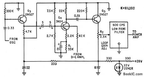
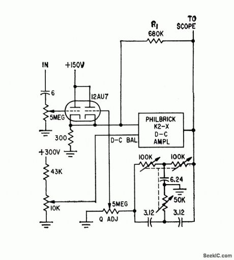
BALANCING_D_C_AMPLIFIER
Published:2009/7/14 20:21:00 Author:May
Gain is 300.Detects slow changes al summing point of operational amplifier, amplifies drift voltage, and provides opposite-polarity output signal for second input grid of operational amplifier, much as in null-seeking servomechanism.-L.S. Klivans, D-C Amplifiers for Control Systems, Electronics, 31:47, p96-100. (View)
View full Circuit Diagram | Comments | Reading(820)
FET_SAMPLE_HOLD_D_C_AMPLIFIER
Published:2009/7/14 20:19:00 Author:May
Has low output impedance for rapid charging of sampling capacitor, unity gain, and no d-c offset adjustment period.-L. J. Sevin, Jr., Field-Effect Transistors, McGraw-Hill, N.Y., 1965,p114. (View)
View full Circuit Diagram | Comments | Reading(910)
VARIABLE_GAIN_INVERTER_AMPLIFIER
Published:2009/7/15 1:58:00 Author:Jessie
Gives gain variations of up to 10 to1, with less than 10% harmonic distortion at 1 v output through use of tetrode transistor, to provide precise voltage regulation of output of d-c to 400-cps a-c inverter. Error current from d-c amplifier of inverter is applied to base 2 of 04, causing ac voltage gain of stage to vary with magnitude of error current..-R.. Wileman, linear Circuits Regulate Solid-State Inverter, Electronics, 33:16, p 61-63. (View)
View full Circuit Diagram | Comments | Reading(824)
TUNABLE_SUBAUDIO_AMPUFIER
Published:2009/7/15 2:03:00 Author:Jessie
Commercial d-c amplifier with twin-T feedback tuningelement tunes from 0.5 to 100 cps, for analyzing low-frequency components of complexwaveforms.-J. IA. Reece, Subaudio Tunable Amplifier, Electronics, 32:45, p 72-74. (View)
View full Circuit Diagram | Comments | Reading(752)
10_W_POWER_AMPLIFIER
Published:2009/7/15 2:02:00 Author:Jessie
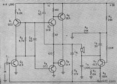
Q1 provides bias current for low-power complementary-symmetry push-pull output stage Q3-Q4, which drives power transistors Q5-Q6. Q7 providesvoltage bias for Q2.-H. W. Parmer, Two Easy Ways to Stabilize Power. Transistor Hill Amplifiers, Electronics, 35:43, p 56-58. (View)
View full Circuit Diagram | Comments | Reading(0)
PHOTOMULTIPLIER_LASER_RECEIVER_WITH_VIDEO_AMPLIFIER_
Published:2009/7/14 12:00:00 Author:May
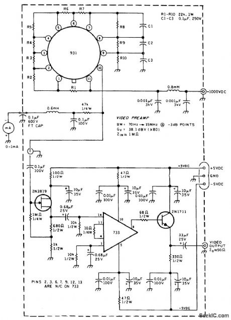
This is a circuit diagram for the inexpensive 931 side-looking PMT and its resistor divider network. This circuit maintains the proper voltages for the dynodes. The capacitors across the last three network resistors improve the frequency response of the PMT to modulated signals. A milliammeter in the PMT anode circuit registers the average PMT current under the medium to high illumination encountered during diagnostic tests. A PMT preamplifier uses a 733 (or equivalent) wideband amplifier. Because the demodulated signal can be either a direct baseband signal or a baseband signal modulated onto a subcarrier, the preamplifier must be capable of amplifying all the demodulated signal frequencies. The preamplifier is designed for a 70-Hz to 15-MHz bandwidth at the -3-dB points and for a gain of 80. Because the signal detection circuits will probably be placed in a separate housing, the video preamplifier is designed to drive a 50-Ω cable. With the high-current multiplication inherent in the PMT, the PMT noise will predominate over the video preamplifier IC noise. (View)
View full Circuit Diagram | Comments | Reading(3671)
IR_REMOTE_CONTROL_REPEATER
Published:2009/7/14 7:41:00 Author:May
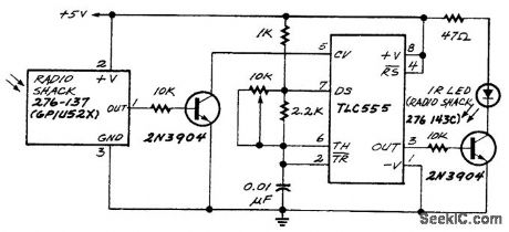
This circuit receives TV remote-control signals and retransmits them. The 555 oscillator provides 40-kHz modulation. The IR LED can be placed in another room. (View)
View full Circuit Diagram | Comments | Reading(851)
ULTRALOW_NOISE_PLAYBACK_PREAMP
Published:2009/7/14 7:39:00 Author:May
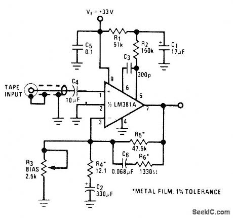
Provides optimum noise performance at popular tape speeds of 1 7/8 and 3 3/4 in/s. Reference gain for 0 dB is 41 dB, giving output level of 200 mV from head output of 1 mV at 1 kHz. Single-ended biasing and use of metal-film resistors reduce noise.- Audio Handbook, National Semiconductor, Santa Clara, CA, 1977, p 2-31-2-37. (View)
View full Circuit Diagram | Comments | Reading(870)
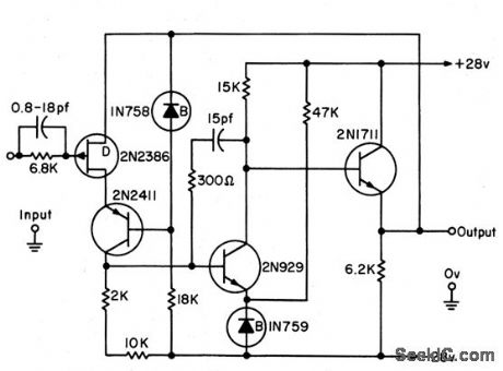
LASER_ACTIVATED_RELAY_WITH_AMPLIFIER
Published:2009/7/14 11:30:00 Author:May
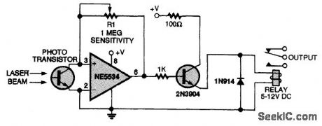
A low-noise amplifier is used in conjunction with a phototransistor to allow higher sensitivity than the detector alone would provide. (View)
View full Circuit Diagram | Comments | Reading(917)
COMMON_BASE_UHF_AMPLIFIER_OR_DOUBLER
Published:2009/7/15 2:51:00 Author:Jessie
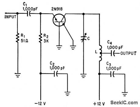
With output tank circuit tuned to frequency input, power gain ranges between 10 and 16 db for 40 to 1,000 Mc, with band-width varying from 10 to 40 Mc depending on temperature, frequency, and loading. Tuning tank to twice input frequency gives frequency doubler.-A. E. Munich, Basic UHF Circuit Forms Amplifiers and Multipliers, Electronics, 37:20, p 59-60. (View)
View full Circuit Diagram | Comments | Reading(1264)
45_W_SERIES_TYPE_POWER_AMPLIFIER
Published:2009/7/15 2:47:00 Author:Jessie
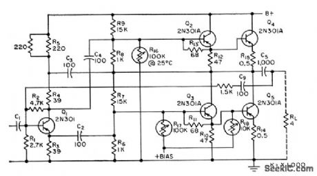
Uses split-load phase inverter, capacitance-coupled to common-collector class B driver,which in turn is direct-coupled to class-B common-emitter output stage. Driver and output stages are each in series for d-c collector supply. No transformers are required.-M. B.Herscher, Designing Transistor A-F Power Amplifiers, Electronics, 31:15, p 96-99. (View)
View full Circuit Diagram | Comments | Reading(1099)
NAB_TAPE_PREAMP
Published:2009/7/14 8:01:00 Author:May
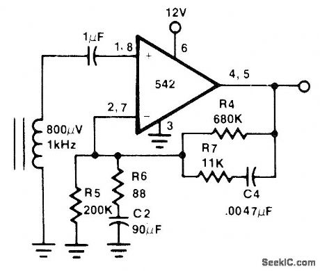
One section of Signetics NE542 dual noise amplifier is used to provide 100-mV output level at 1 kHz following NAB equalization curve for tape speed of 7 1/2 in/s.- Signetics Analog Data Manual, Signetics, Sunnyvale, CA, 1977, p 780. (View)
View full Circuit Diagram | Comments | Reading(2083)
12_V_PLAYBACK_PREAMP
Published:2009/7/14 7:56:00 Author:May
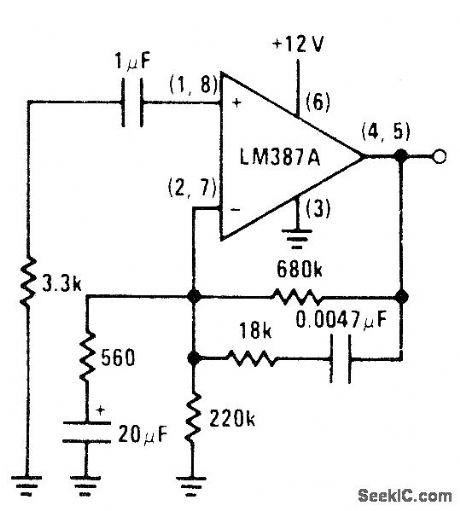
Provides standard NAB equalization Gain is decreased gradually from 60 dB at 20 Hz to 32 dB at 20 kHz in accordance with NAB playback curve Playback head is represented by 3.3K resistor.- Audio Hand-book, National Semiconductor, Santa Clara, CA, 1977, p 2-31-2-37.
(View)
View full Circuit Diagram | Comments | Reading(855)
PREFERRED_AUDIO_POWER_AMPLIFIER
Published:2009/7/15 2:36:00 Author:Jessie
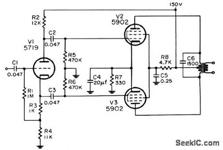
Delivers 2 w with less than 5% distortion to suitably matched load. If push-Pull tubes are dynamically matched, screen and cathode bypass capacitors C4 and C5 may be omitted. -NBS, Handbook Preferred Circuits Navy Aeronautical Electronic Equipment, Vol. I, Electron Tube Circuits, 1963, PC 64, p 64-2. (View)
View full Circuit Diagram | Comments | Reading(3954)
DIGITAL_CASSETTE_READ_AMPLIFIER
Published:2009/7/14 6:46:00 Author:May
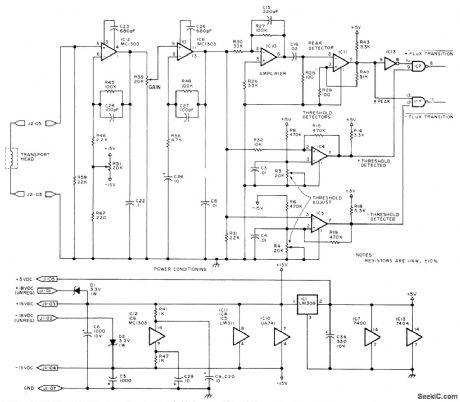
Signal from magnetic head of digital tape cassette is amplified by two-stage MC1303 amplifier providing analog output of about 4 V P-P to μA741 opamp IC10 of LM311 peak detector 1C11. Signal also goes to LM311 positive and negative threshold detectors is low; above reference, output is high. Negative threshold detector operates similarly for negative pulses. Time jitter in outputs is eliminated by detecting peak of analog read signal, then combining result with threshold in. formation in peak detector. Circuit is used ; Phi-Deck cassette system made by Economy Company, Oklahoma City.-I, Rampil and J. Breimeir, The Digital Cassette Subsystem: Dig-ital Recording Background and Head Interface Electronics, BYTE, Feb. 1977, p 24-31. (View)
View full Circuit Diagram | Comments | Reading(1688)
| Pages:69/250 At 206162636465666768697071727374757677787980Under 20 |
Circuit Categories
power supply circuit
Amplifier Circuit
Basic Circuit
LED and Light Circuit
Sensor Circuit
Signal Processing
Electrical Equipment Circuit
Control Circuit
Remote Control Circuit
A/D-D/A Converter Circuit
Audio Circuit
Measuring and Test Circuit
Communication Circuit
Computer-Related Circuit
555 Circuit
Automotive Circuit
Repairing Circuit